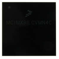
MCIMX31LCVMN4C Freescale Semiconductor, MCIMX31LCVMN4C Datasheet - Page 17

MCIMX31LCVMN4C
Manufacturer Part Number
MCIMX31LCVMN4C
Description
IC MPU MAP I.MX31L 473-MAPBGA
Manufacturer
Freescale Semiconductor
Series
i.MX31r
Specifications of MCIMX31LCVMN4C
Core Processor
ARM11
Core Size
32-Bit
Speed
400MHz
Connectivity
1-Wire, ATA, EBI/EMI, FIR, I²C, MMC/SD, PCMCIA, SIM, SPI, SSI, UART/USART, USB, USB OTG
Peripherals
DMA, LCD, POR, PWM, WDT
Program Memory Type
ROMless
Ram Size
16K x 8
Voltage - Supply (vcc/vdd)
1.22 V ~ 3.3 V
Oscillator Type
External
Operating Temperature
-40°C ~ 85°C
Package / Case
473-MAPBGA
Lead Free Status / RoHS Status
Lead free / RoHS Compliant
Number Of I /o
-
Eeprom Size
-
Program Memory Size
-
Data Converters
-
Available stocks
Company
Part Number
Manufacturer
Quantity
Price
Company:
Part Number:
MCIMX31LCVMN4C
Manufacturer:
Freescale Semiconductor
Quantity:
10 000
Company:
Part Number:
MCIMX31LCVMN4CR2
Manufacturer:
Freescale Semiconductor
Quantity:
10 000
1
Freescale Semiconductor
High-level output voltage
Low-level output voltage
High-level output current, slow slew rate
High-level output current, fast slew rate
Low-level output current, slow slew rate
Low-level output current, fast slew rate
High-Level DC input voltage
Low-Level DC input voltage
Input Hysteresis
Schmitt trigger VT+
Schmitt trigger VT–
Pull-up resistor (100 kΩ PU)
Pull-down resistor (100 kΩ PD)
Input current (no PU/PD)
Input current (100 kΩ PU)
Input current (100 kΩ PD)
Tri-state leakage current
Not a precise value. Measurements made on small sample size have shown variations of ±50% or more.
Parameter
The term NVCC in this section refers to the associated supply rail of an
input or output. The association is shown in the Signal Multiplexing chapter
of the reference manual. NVCC for
NVCC3–10; QVCC refers to QVCC, QVCC1, and QVCC4.
MCIMX31C/MCIMX31LC Technical Data, Rev. 4.3
Table 12. GPIO DC Electrical Parameters
Symbol
I
I
I
I
V
R
R
V
V
V
OH_S
OH_F
V
OL_S
OL_F
V
V
I
I
I
I
HYS
PU
PD
OZ
T
T
OH
IN
IN
IN
OL
IH
IL
+
–
1
1
I
I
OH
Hysteresis enabled
Hysteresis enabled
Hysteresis enabled
V
V
OL
Test Conditions
V
V
I
I
V
V
NOTE
= NVCC or GND
= NVCC or GND
OH
OH
= specified Drive
OL
OL
= specified Drive
I
I/O = High Z
OH
Table 12
I
V
High Drive
High Drive
High Drive
High Drive
Max Drive
Max Drive
Max Drive
Max Drive
OL
Std Drive
Std Drive
Std Drive
Std Drive
=0.2*NVCC
=0.2*NVCC
I
=0.8*NVCC
=0.8*NVCC
V
= NVCC
= –1 mA
= 1 mA
I
—
—
—
—
= 0
refers to NVCC1 and
NVCC –0.15
0.5*QVCC
0.8*NVCC
0.7*NVCC
0.25
Min
—
—
–2
–4
–8
–4
–6
–8
—
—
—
—
—
—
—
2
4
8
4
6
8
0
Typ
100
100
—
—
—
—
—
—
—
—
—
—
—
—
—
—
—
—
—
Electrical Characteristics
0.2*NVCC
0.3*QVCC
0.5*QVCC
NVCC
0.15
Max
25
28
—
—
—
—
—
—
—
—
—
—
±1
±2
Units
mA
mA
mA
mA
kΩ
μA
μA
μA
μA
μA
V
V
V
V
V
V
V
V
V
17


