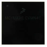
MCIMX31LCVMN4C Freescale Semiconductor, MCIMX31LCVMN4C Datasheet - Page 57

MCIMX31LCVMN4C
Manufacturer Part Number
MCIMX31LCVMN4C
Description
IC MPU MAP I.MX31L 473-MAPBGA
Manufacturer
Freescale Semiconductor
Series
i.MX31r
Specifications of MCIMX31LCVMN4C
Core Processor
ARM11
Core Size
32-Bit
Speed
400MHz
Connectivity
1-Wire, ATA, EBI/EMI, FIR, I²C, MMC/SD, PCMCIA, SIM, SPI, SSI, UART/USART, USB, USB OTG
Peripherals
DMA, LCD, POR, PWM, WDT
Program Memory Type
ROMless
Ram Size
16K x 8
Voltage - Supply (vcc/vdd)
1.22 V ~ 3.3 V
Oscillator Type
External
Operating Temperature
-40°C ~ 85°C
Package / Case
473-MAPBGA
Lead Free Status / RoHS Status
Lead free / RoHS Compliant
Number Of I /o
-
Eeprom Size
-
Program Memory Size
-
Data Converters
-
Available stocks
Company
Part Number
Manufacturer
Quantity
Price
Company:
Part Number:
MCIMX31LCVMN4C
Manufacturer:
Freescale Semiconductor
Quantity:
10 000
Company:
Part Number:
MCIMX31LCVMN4CR2
Manufacturer:
Freescale Semiconductor
Quantity:
10 000
1
2
Tdicd
IP16 Display interface clock low time
IP17 Display interface clock high
IP18 Data setup time
IP19 Data holdup time
IP20 Control signals setup time to
The SCREEN_WIDTH, SCREEN_HEIGHT, H_SYNC_WIDTH, V_SYNC_WIDTH, BGXP, BGYP and
V_SYNC_WIDTH_L parameters are programmed via the SDC_HOR_CONF, SDC_VER_CONF,
SDC_BG_POS Registers. The FW and FH parameters are programmed for the corresponding DMA
channel. The DISP3_IF_CLK_PER_WR, HSP_CLK_PERIOD and DISP3_IF_CLK_CNT_D parameters
are programmed via the DI_DISP3_TIME_CONF, DI_HSP_CLK_PER and DI_DISP_ACC_CC
Registers.
Figure 48
parameters. The DISP3_IF_CLK_DOWN_WR and DISP3_IF_CLK_UP_WR parameters are set via the
DI_DISP3_TIME_CONF Register.
Freescale Semiconductor
ID
The exact conditions have not been finalized, but will likely match the current customer requirement for their specific display. These
conditions may be device specific.
Display interface clock down time
time
display interface clock
=
DISPB_D3_VSYNC
DISPB_D3_HSYNC
DISPB_D3_DRDY
1
-- - T
2
DISPB_D3_CLK
HSP_CLK
depicts the synchronous display interface timing for access level, and
other controls
DISPB_DATA
Parameter
HSP_CLK is the High-Speed Port Clock, which is the input to the Image
Processing Unit (IPU). Its frequency is controlled by the Clock Control
Module (CCM) settings. The HSP_CLK frequency must be greater than or
equal to the AHB clock frequency.
Table 45. Synchronous Display Interface Timing Parameters—Access Level
Figure 48. Synchronous Display Interface Timing Diagram—Access Level
⋅
ceil
2 DISP3_IF_CLK_DOWN_WR
-------------------------------------------------------------------------------- -
⋅
IP16
HSP_CLK_PERIOD
MCIMX31C/MCIMX31LC Technical Data, Rev. 4.3
Symbol
Tdsu
Tdhd
Tckh
Tcsu
Tckl
IP17
Tdicd–Tdicu–1.5
Tdicp–Tdicd+Tdicu–1.5
Tdicd–3.5
Tdicp–Tdicd–3.5
Tdicd–3.5
IP19
Min
NOTE
IP18
IP20
Tdicu
Tdicd
Tdicp–Tdicd+Tdicu
Tdicu
Tdicp–Tdicu
2
–Tdicu
Typ
1
3
Tdicd–Tdicu+1.5
Tdicp–Tdicd+Tdicu+1.5
Table 45
Electrical Characteristics
Max
—
—
—
lists the timing
Units
ns
ns
ns
ns
ns
57


