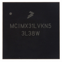
MCIMX31LVKN5 Freescale Semiconductor, MCIMX31LVKN5 Datasheet - Page 10

MCIMX31LVKN5
Manufacturer Part Number
MCIMX31LVKN5
Description
IC MPU MAP I.MX31L 457-MAPBGA
Manufacturer
Freescale Semiconductor
Series
i.MX31r
Datasheet
1.MCIMX31LITEKITC.pdf
(122 pages)
Specifications of MCIMX31LVKN5
Core Processor
ARM11
Core Size
32-Bit
Speed
532MHz
Connectivity
1-Wire, ATA, EBI/EMI, FIR, I²C, MMC/SD, PCMCIA, SIM, SPI, SSI, UART/USART, USB, USB OTG
Peripherals
DMA, LCD, POR, PWM, WDT
Program Memory Type
ROMless
Ram Size
16K x 8
Voltage - Supply (vcc/vdd)
1.22 V ~ 3.3 V
Oscillator Type
External
Operating Temperature
0°C ~ 70°C
Package / Case
457-MAPBGA
Lead Free Status / RoHS Status
Lead free / RoHS Compliant
Number Of I /o
-
Eeprom Size
-
Program Memory Size
-
Data Converters
-
Available stocks
Company
Part Number
Manufacturer
Quantity
Price
Company:
Part Number:
MCIMX31LVKN5
Manufacturer:
ADI
Quantity:
9 710
Company:
Part Number:
MCIMX31LVKN5
Manufacturer:
Freescale Semiconductor
Quantity:
10 000
Company:
Part Number:
MCIMX31LVKN5B
Manufacturer:
Freescale Semiconductor
Quantity:
10 000
Company:
Part Number:
MCIMX31LVKN5BR2
Manufacturer:
Freescale Semiconductor
Quantity:
10 000
Company:
Part Number:
MCIMX31LVKN5C
Manufacturer:
FREESCALE
Quantity:
1 831
Company:
Part Number:
MCIMX31LVKN5C
Manufacturer:
FREESCALE
Quantity:
748
Company:
Part Number:
MCIMX31LVKN5C
Manufacturer:
Freescale Semiconductor
Quantity:
10 000
Part Number:
MCIMX31LVKN5C
Manufacturer:
FREESCALE
Quantity:
20 000
Company:
Part Number:
MCIMX31LVKN5R2
Manufacturer:
IBM
Quantity:
284
Part Number:
MCIMX31LVKN5R2
Manufacturer:
FREESCALE
Quantity:
20 000
Electrical Characteristics
4
This section provides the device-level and module-level electrical characteristics for the MCIMX31.
4.1
This section provides the device-level electrical characteristics for the IC. See
to the individual tables and sections.
10
1
Supply Voltage (Core)
Supply Voltage (I/O)
Input Voltage Range
Storage Temperature
ESD Damage Immunity:
Offset voltage allowed in run mode between core supplies.
The offset is the difference between all core voltage pair combinations of QVCC, QVCC1, and QVCC4.
Electrical Characteristics
Chip-Level Conditions
Table 5, “Absolute Maximum Ratings”
Table
Table 8, “Operating Ranges”
Table
Table 10, “Interface Frequency”
Section 4.1.1, “Supply Current Specifications”
Section 4.2, “Supply Power-Up/Power-Down Requirements and Restrictions”
Stresses beyond those listed under
the device. These are stress ratings only. Functional operation of the device
at these or any other conditions beyond those indicated under
"Operating Ranges," on page 13
absolute-maximum-rated conditions for extended periods may affect device
reliability.
7, “Thermal Resistance Data—19 × 19 mm Package”
9,
“Specific Operating Ranges for Silicon Revision 2.0”
Parameter
Charge Device Model (CDM)
For these characteristics, …
Table 4. MCIMX31 Chip-Level Conditions
Human Body Model (HBM)
MCIMX31/MCIMX31L Technical Data, Rev. 4.1
Table 5. Absolute Maximum Ratings
Machine Model (MM)
CAUTION
is not implied. Exposure to
Table 5
may cause permanent damage to
V
QVCC
NVCC
Symbol
core_offset
T
V
storage
V
Imax
esd
max
max
1
–0.5
–0.5
–0.5
Min
–40
—
—
—
—
Table 4
Table 8,
Topic appears …
on page 10
on page 11
on page 13
on page 14
on page 14
on page 16
on page 19
NVCC +0.3
Freescale Semiconductor
for a quick reference
1500
Max
1.65
125
200
500
3.3
15
Units
mV
o
V
V
V
V
C


