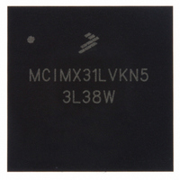
MCIMX31LVKN5 Freescale Semiconductor, MCIMX31LVKN5 Datasheet - Page 26

MCIMX31LVKN5
Manufacturer Part Number
MCIMX31LVKN5
Description
IC MPU MAP I.MX31L 457-MAPBGA
Manufacturer
Freescale Semiconductor
Series
i.MX31r
Datasheet
1.MCIMX31LITEKITC.pdf
(122 pages)
Specifications of MCIMX31LVKN5
Core Processor
ARM11
Core Size
32-Bit
Speed
532MHz
Connectivity
1-Wire, ATA, EBI/EMI, FIR, I²C, MMC/SD, PCMCIA, SIM, SPI, SSI, UART/USART, USB, USB OTG
Peripherals
DMA, LCD, POR, PWM, WDT
Program Memory Type
ROMless
Ram Size
16K x 8
Voltage - Supply (vcc/vdd)
1.22 V ~ 3.3 V
Oscillator Type
External
Operating Temperature
0°C ~ 70°C
Package / Case
457-MAPBGA
Lead Free Status / RoHS Status
Lead free / RoHS Compliant
Number Of I /o
-
Eeprom Size
-
Program Memory Size
-
Data Converters
-
Available stocks
Company
Part Number
Manufacturer
Quantity
Price
Company:
Part Number:
MCIMX31LVKN5
Manufacturer:
ADI
Quantity:
9 710
Company:
Part Number:
MCIMX31LVKN5
Manufacturer:
Freescale Semiconductor
Quantity:
10 000
Company:
Part Number:
MCIMX31LVKN5B
Manufacturer:
Freescale Semiconductor
Quantity:
10 000
Company:
Part Number:
MCIMX31LVKN5BR2
Manufacturer:
Freescale Semiconductor
Quantity:
10 000
Company:
Part Number:
MCIMX31LVKN5C
Manufacturer:
FREESCALE
Quantity:
1 831
Company:
Part Number:
MCIMX31LVKN5C
Manufacturer:
FREESCALE
Quantity:
748
Company:
Part Number:
MCIMX31LVKN5C
Manufacturer:
Freescale Semiconductor
Quantity:
10 000
Part Number:
MCIMX31LVKN5C
Manufacturer:
FREESCALE
Quantity:
20 000
Company:
Part Number:
MCIMX31LVKN5R2
Manufacturer:
IBM
Quantity:
284
Part Number:
MCIMX31LVKN5R2
Manufacturer:
FREESCALE
Quantity:
20 000
Electrical Characteristics
4.3.4
Figure 7
Figure 8
Figure 9
the timing parameters.
26
1-Wire bus
(BATT_LINE)
OW1
OW2
OW3
OW4
ID
OW5
OW6
depicts Write 1 Sequence timing,
depicts the RPP timing, and
depicts Write 0 Sequence timing, and
ID
1-Wire Electrical Specifications
(BATT_LINE)
1-Wire bus
Write 0 Low Time
Transmission Time Slot
Table 21. RPP Sequence Delay Comparisons Timing Parameters
Figure 7. Reset and Presence Pulses (RPP) Timing Diagram
Presence Detect High
Presence Detect Low
Reset Time High
Reset Time Low
Parameters
Parameter
“Reset Pulse”
OWIRE Tx
Table 22. WR0 Sequence Timing Parameters
Figure 8. Write 0 Sequence Timing Diagram
MCIMX31/MCIMX31L Technical Data, Rev. 4.1
OW1
Table 21
Figure 10
lists the RPP timing parameters.
Table 22
OW5
t
Symbol
WR0_low
depicts the Read Sequence timing, and
t
SLOT
Symbol
t
t
t
t
RSTH
RSTL
PDH
PDL
lists the timing parameters.
OW6
OW3
OW2
OW5
Min
60
“Presence Pulse”
Min
480
480
15
60
DS2502 Tx
Typ
100
117
Typ
511
512
—
—
OW4
Freescale Semiconductor
Max
120
120
Max
240
60
—
—
Table 23
Units
Units
µs
µs
µs
µs
µs
µs
lists


