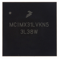
MCIMX31LVKN5 Freescale Semiconductor, MCIMX31LVKN5 Datasheet - Page 78

MCIMX31LVKN5
Manufacturer Part Number
MCIMX31LVKN5
Description
IC MPU MAP I.MX31L 457-MAPBGA
Manufacturer
Freescale Semiconductor
Series
i.MX31r
Datasheet
1.MCIMX31LITEKITC.pdf
(122 pages)
Specifications of MCIMX31LVKN5
Core Processor
ARM11
Core Size
32-Bit
Speed
532MHz
Connectivity
1-Wire, ATA, EBI/EMI, FIR, I²C, MMC/SD, PCMCIA, SIM, SPI, SSI, UART/USART, USB, USB OTG
Peripherals
DMA, LCD, POR, PWM, WDT
Program Memory Type
ROMless
Ram Size
16K x 8
Voltage - Supply (vcc/vdd)
1.22 V ~ 3.3 V
Oscillator Type
External
Operating Temperature
0°C ~ 70°C
Package / Case
457-MAPBGA
Lead Free Status / RoHS Status
Lead free / RoHS Compliant
Number Of I /o
-
Eeprom Size
-
Program Memory Size
-
Data Converters
-
Available stocks
Company
Part Number
Manufacturer
Quantity
Price
Company:
Part Number:
MCIMX31LVKN5
Manufacturer:
ADI
Quantity:
9 710
Company:
Part Number:
MCIMX31LVKN5
Manufacturer:
Freescale Semiconductor
Quantity:
10 000
Company:
Part Number:
MCIMX31LVKN5B
Manufacturer:
Freescale Semiconductor
Quantity:
10 000
Company:
Part Number:
MCIMX31LVKN5BR2
Manufacturer:
Freescale Semiconductor
Quantity:
10 000
Company:
Part Number:
MCIMX31LVKN5C
Manufacturer:
FREESCALE
Quantity:
1 831
Company:
Part Number:
MCIMX31LVKN5C
Manufacturer:
FREESCALE
Quantity:
748
Company:
Part Number:
MCIMX31LVKN5C
Manufacturer:
Freescale Semiconductor
Quantity:
10 000
Part Number:
MCIMX31LVKN5C
Manufacturer:
FREESCALE
Quantity:
20 000
Company:
Part Number:
MCIMX31LVKN5R2
Manufacturer:
IBM
Quantity:
284
Part Number:
MCIMX31LVKN5R2
Manufacturer:
FREESCALE
Quantity:
20 000
Electrical Characteristics
The DISP#_IF_CLK_PER_WR, DISP#_IF_CLK_PER_RD, HSP_CLK_PERIOD,
DISP#_IF_CLK_DOWN_WR, DISP#_IF_CLK_UP_WR, DISP#_IF_CLK_DOWN_RD,
DISP#_IF_CLK_UP_RD and DISP#_READ_EN parameters are programmed via the
DI_DISP#_TIME_CONF_1, DI_DISP#_TIME_CONF_2 and DI_HSP_CLK_PER Registers.
4.3.15.5.3
The IPU supports the following types of asynchronous serial interfaces:
Figure 61
DISPB_D#_CS signal and the straight polarity of the DISPB_SD_D_CLK signal.
For this interface, a bidirectional data line is used outside the device. The IPU still uses separate input and
output data lines (IPP_IND_DISPB_SD_D and IPP_DO_DISPB_SD_D). The I/O mux should provide
joining the internal data lines to the bidirectional external line according to the IPP_OBE_DISPB_SD_D
signal provided by the IPU.
Each data transfer can be preceded by an optional preamble with programmable length and contents. The
preamble is followed by read/write (RW) and address (RS) bits. The order of the these bits is
programmable. The RW bit can be disabled. The following data can consist of one word or of a whole
burst. The interface parameters are controlled by the DI_SER_DISP1_CONF and DI_SER_DISP2_CONF
Registers.
Figure 62
data lines both inside and outside the device.
78
DISPB_SD_D_CLK
DISPB_D#_CS
DISPB_SD_D
•
•
•
•
3-wire (with bidirectional data line)
4-wire (with separate data input and output lines)
5-wire type 1 (with sampling RS by the serial clock)
5-wire type 2 (with sampling RS by the chip select signal)
depicts timing of the 4-wire serial interface. For this interface, there are separate input and output
depicts timing of the 3-wire serial interface. The timing images correspond to active-low
Serial Interfaces
1 display IF
clock cycle
Figure 61. 3-Wire Serial Interface Timing Diagram
Preamble
MCIMX31/MCIMX31L Technical Data, Rev. 4.1
, Functional Description
RW
RS
D7
D6
D5
Input or output data
D4
D3
Freescale Semiconductor
D2
1 display IF
clock cycle
D1
D0


