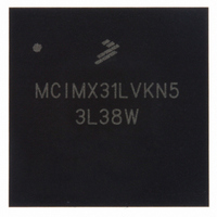
MCIMX31LVKN5 Freescale Semiconductor, MCIMX31LVKN5 Datasheet - Page 53

MCIMX31LVKN5
Manufacturer Part Number
MCIMX31LVKN5
Description
IC MPU MAP I.MX31L 457-MAPBGA
Manufacturer
Freescale Semiconductor
Series
i.MX31r
Datasheet
1.MCIMX31LITEKITC.pdf
(122 pages)
Specifications of MCIMX31LVKN5
Core Processor
ARM11
Core Size
32-Bit
Speed
532MHz
Connectivity
1-Wire, ATA, EBI/EMI, FIR, I²C, MMC/SD, PCMCIA, SIM, SPI, SSI, UART/USART, USB, USB OTG
Peripherals
DMA, LCD, POR, PWM, WDT
Program Memory Type
ROMless
Ram Size
16K x 8
Voltage - Supply (vcc/vdd)
1.22 V ~ 3.3 V
Oscillator Type
External
Operating Temperature
0°C ~ 70°C
Package / Case
457-MAPBGA
Lead Free Status / RoHS Status
Lead free / RoHS Compliant
Number Of I /o
-
Eeprom Size
-
Program Memory Size
-
Data Converters
-
Available stocks
Company
Part Number
Manufacturer
Quantity
Price
Company:
Part Number:
MCIMX31LVKN5
Manufacturer:
ADI
Quantity:
9 710
Company:
Part Number:
MCIMX31LVKN5
Manufacturer:
Freescale Semiconductor
Quantity:
10 000
Company:
Part Number:
MCIMX31LVKN5B
Manufacturer:
Freescale Semiconductor
Quantity:
10 000
Company:
Part Number:
MCIMX31LVKN5BR2
Manufacturer:
Freescale Semiconductor
Quantity:
10 000
Company:
Part Number:
MCIMX31LVKN5C
Manufacturer:
FREESCALE
Quantity:
1 831
Company:
Part Number:
MCIMX31LVKN5C
Manufacturer:
FREESCALE
Quantity:
748
Company:
Part Number:
MCIMX31LVKN5C
Manufacturer:
Freescale Semiconductor
Quantity:
10 000
Part Number:
MCIMX31LVKN5C
Manufacturer:
FREESCALE
Quantity:
20 000
Company:
Part Number:
MCIMX31LVKN5R2
Manufacturer:
IBM
Quantity:
284
Part Number:
MCIMX31LVKN5R2
Manufacturer:
FREESCALE
Quantity:
20 000
Freescale Semiconductor
1
SD17
SD18
SD19
SD20
Test condition: Measured using delay line 5 programmed as follows: ESDCDLY5[15:0] = 0x0703.
ID
DQM (output)
DQS (output)
DQ (output)
DQ and DQM setup time to DQS
DQ and DQM hold time to DQS
Write cycle DQS falling edge to SDCLK output delay time.
Write cycle DQS falling edge to SDCLK output hold time.
SDCLK
SDCLK
SDRAM CLK and DQS related parameters are being measured from the
50% point—that is, high is defined as 50% of signal value and low is defined
as 50% of signal value.
The timing parameters are similar to the ones used in SDRAM data
sheets—that is,
are driven by the ESDCTL at the negative edge of SDCLK and the
parameters are measured at maximum memory frequency.
Table 38. Mobile DDR SDRAM Write Cycle Timing Parameters
Figure 38. Mobile DDR SDRAM Write Cycle Timing Diagram
SD17
Table 38
SD17
MCIMX31/MCIMX31L Technical Data, Rev. 4.1
Parameter
Data
DM
indicates SDRAM requirements. All output signals
SD18
SD18
Data
DM
NOTE
Data
SD17
DM
SD17
Data
DM
SD18
SD18
Data
DM
Symbol
tDSS
tDSH
tDH
tDS
Data
DM
SD19
1
Electrical Characteristics
0.95
0.95
Data
DM
Min
1.8
1.8
SD20
Max
—
—
—
—
Data
DM
Unit
ns
ns
ns
ns
53


