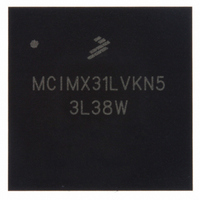
MCIMX31LVKN5 Freescale Semiconductor, MCIMX31LVKN5 Datasheet - Page 20

MCIMX31LVKN5
Manufacturer Part Number
MCIMX31LVKN5
Description
IC MPU MAP I.MX31L 457-MAPBGA
Manufacturer
Freescale Semiconductor
Series
i.MX31r
Datasheet
1.MCIMX31LITEKITC.pdf
(122 pages)
Specifications of MCIMX31LVKN5
Core Processor
ARM11
Core Size
32-Bit
Speed
532MHz
Connectivity
1-Wire, ATA, EBI/EMI, FIR, I²C, MMC/SD, PCMCIA, SIM, SPI, SSI, UART/USART, USB, USB OTG
Peripherals
DMA, LCD, POR, PWM, WDT
Program Memory Type
ROMless
Ram Size
16K x 8
Voltage - Supply (vcc/vdd)
1.22 V ~ 3.3 V
Oscillator Type
External
Operating Temperature
0°C ~ 70°C
Package / Case
457-MAPBGA
Lead Free Status / RoHS Status
Lead free / RoHS Compliant
Number Of I /o
-
Eeprom Size
-
Program Memory Size
-
Data Converters
-
Available stocks
Company
Part Number
Manufacturer
Quantity
Price
Company:
Part Number:
MCIMX31LVKN5
Manufacturer:
ADI
Quantity:
9 710
Company:
Part Number:
MCIMX31LVKN5
Manufacturer:
Freescale Semiconductor
Quantity:
10 000
Company:
Part Number:
MCIMX31LVKN5B
Manufacturer:
Freescale Semiconductor
Quantity:
10 000
Company:
Part Number:
MCIMX31LVKN5BR2
Manufacturer:
Freescale Semiconductor
Quantity:
10 000
Company:
Part Number:
MCIMX31LVKN5C
Manufacturer:
FREESCALE
Quantity:
1 831
Company:
Part Number:
MCIMX31LVKN5C
Manufacturer:
FREESCALE
Quantity:
748
Company:
Part Number:
MCIMX31LVKN5C
Manufacturer:
Freescale Semiconductor
Quantity:
10 000
Part Number:
MCIMX31LVKN5C
Manufacturer:
FREESCALE
Quantity:
20 000
Company:
Part Number:
MCIMX31LVKN5R2
Manufacturer:
IBM
Quantity:
284
Part Number:
MCIMX31LVKN5R2
Manufacturer:
FREESCALE
Quantity:
20 000
Electrical Characteristics
4.2.1.1
Silicon revision 2.0 offers two options for power-up sequencing. Option 1 is backwards compatible with
silicon revision 1.2 and earlier versions of the IC. It should be noted that using option 1 on silicon Rev. 2.0
introduces a slight increase in current drain on IOQVDD when IOQVDD is raised before NVCC21. The
expected resulting increase is in the range of 3 mA to 5 mA, which does not pose a risk to the IC.
Option 2 is an alternative power-up sequence that allows the powering up of NVCC2, NVCC21, NVCC22
with IOQVDD, NVCC1, and NVCC3-10 without producing a current drain increase on IOQVDD.
These two power-up options on the 2.0 silicon allow the user to select the optimum power-up sequence for
their application.
20
FUSE_VDD
Power-Up Sequence for Silicon Revision 2
IOQVDD, NVCC1, NVCC3–10
NVCC2, NVCC21, NVCC22
QVCC, QVCC1, QVCC4
1, 3
Hold POR Asserted
Figure 2. Power-Up Sequence for Silicon Revisions 1.2 and Previous
Release POR
1
MCIMX31/MCIMX31L Technical Data, Rev. 4.1
FVCC, MVCC,
SVCC, UVCC
1
1, 2
1
Notes:
1
2
3
1
The board design must guarantee that supplies reach 90% level before transition
to the next state, using Power Management IC or other means.
The NVCC1 supply must not precede IOQVDD by more than 0.2 V until IOQVDD
has reached 1.5 V. If IOQVDD is powered up first, there are no restrictions.
It is allowable for FVCC, MVCC, SVCC, and UVCC to be up after FUSE_VDD.
Freescale Semiconductor


