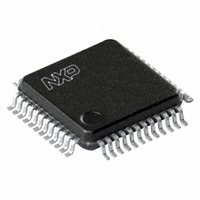
SC68C652BIB48,157 NXP Semiconductors, SC68C652BIB48,157 Datasheet - Page 15

SC68C652BIB48,157
Manufacturer Part Number
SC68C652BIB48,157
Description
IC UART DUAL 48LQFP
Manufacturer
NXP Semiconductors
Datasheet
1.SC68C652BIB48128.pdf
(43 pages)
Specifications of SC68C652BIB48,157
Features
2 Channels
Number Of Channels
2, DUART
Fifo's
32 Byte
Voltage - Supply
2.5V, 3.3V, 5V
With Auto Flow Control
Yes
With Irda Encoder/decoder
Yes
With False Start Bit Detection
Yes
With Modem Control
Yes
Mounting Type
Surface Mount
Package / Case
48-LFQFP
Voltage
2.25 V ~ 5.5 V
Lead Free Status / RoHS Status
Lead free / RoHS Compliant
Other names
935278766157
SC68C652BIB48
SC68C652BIB48
SC68C652BIB48
SC68C652BIB48
Available stocks
Company
Part Number
Manufacturer
Quantity
Price
Company:
Part Number:
SC68C652BIB48,157
Manufacturer:
NXP Semiconductors
Quantity:
10 000
NXP Semiconductors
7. Register descriptions
Table 9.
[1]
[2]
[3]
[4]
[5]
SC68C652B_2
Product data sheet
A2 A1 A0 Register Default
General register set
0
0
0
0
0
0
1
1
1
1
Special register set
0
0
Enhanced register set
0
1
1
1
1
The value shown in represents the register’s initialized hexadecimal value; X = not applicable.
Accessible only when LCR[7] is logic 0.
These bits are only accessible when EFR[4] is set.
Baud rate registers accessible only when LCR[7] is logic 1.
Enhanced Feature Register, Xon1/Xon2 and Xoff1/Xoff2 are accessible only when LCR is set to ‘BFh’.
0
0
0
1
1
1
0
0
1
1
0
0
1
0
0
1
1
0
0
1
0
0
1
0
1
0
1
0
1
0
0
1
0
1
SC68C652B internal registers
RHR
THR
IER
FCR
ISR
LCR
MCR
LSR
MSR
SPR
DLL
DLM
EFR
Xon1
Xon2
Xoff1
Xoff2
[4]
[2]
[5]
XX
XX
00
00
01
00
00
60
X0
FF
XX
XX
00
00
00
00
00
Table 9
assigned bit functions are more fully defined in
[1]
details the assigned bit functions for the SC68C652B internal registers. The
Bit 7
bit 7
bit 7
CTS
interrupt
[3]
RCVR
trigger
(MSB)
FIFOs
enabled
divisor
latch
enable
clock
select
FIFO
data
error
CD
bit 7
bit 7
bit 15
Auto-
CTS
bit 7
bit 15
bit 7
bit 15
[3]
Bit 6
bit 6
bit 6
RTS
interrupt
[3]
RCVR
trigger
(LSB)
FIFOs
enabled
set break set parity even
IRDA
enable
THR and
TSR
empty
RI
bit 6
bit 6
bit 14
Auto-
RTS
bit 6
bit 14
bit 6
bit 14
Rev. 02 — 2 November 2009
Dual UART with 32-byte FIFOs and IrDA encoder/decoder
Bit 5
bit 5
bit 5
Xoff
interrupt
[3]
TX
trigger
(MSB)
INT
priority
bit 4
0
THR
empty
DSR
bit 5
bit 5
bit 13
Special
character
detect
bit 5
bit 13
bit 5
bit 13
[3]
Bit 4
bit 4
bit 4
Sleep
mode
TX
trigger
(LSB)
INT
priority
bit 3
parity
loopback OP2
break
interrupt
CTS
bit 4
bit 4
bit 12
Enable
IER[4:7],
ISR[4:5],
FCR[4:5],
MCR[5:7]
bit 4
bit 12
bit 4
bit 12
[3]
[3]
Section 7.1
Bit 3
bit 3
bit 3
modem
status
interrupt
RX
DMA
mode
select
INT
priority
bit 2
parity
enable
control
framing
error
bit 3
bit 3
bit 11
Cont-3
TX, RX
Control
bit 3
bit 11
bit 3
bit 11
CD
through
Bit 2
bit 2
bit 2
receive
line
status
interrupt
XMIT
FIFO
reset
INT
priority
bit 1
stop bits word
(OP1)
parity
error
bit 2
bit 2
bit 10
Cont-2
TX, RX
Control
bit 2
bit 10
bit 2
bit 10
RI
SC68C652B
Section
© NXP B.V. 2009. All rights reserved.
Bit 1
bit 1
bit 1
transmit
holding
register
interrupt
RCVR
FIFO
reset
INT
priority
bit 0
length
bit 1
RTS
overrun
error
bit 1
bit 1
bit 9
Cont-1
TX, RX
Control
bit 1
bit 9
bit 1
bit 9
DSR
7.11.
Bit 0
bit 0
bit 0
receive
holding
register
FIFOs
enable
INT
status
word
length
bit 0
DTR
receive
data
ready
bit 0
bit 0
bit 8
Cont-0
TX, RX
Control
bit 0
bit 8
bit 0
bit 8
CTS
15 of 43


