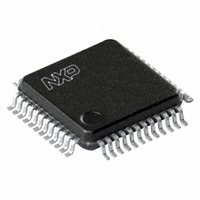
SC68C652BIB48,157 NXP Semiconductors, SC68C652BIB48,157 Datasheet - Page 5

SC68C652BIB48,157
Manufacturer Part Number
SC68C652BIB48,157
Description
IC UART DUAL 48LQFP
Manufacturer
NXP Semiconductors
Datasheet
1.SC68C652BIB48128.pdf
(43 pages)
Specifications of SC68C652BIB48,157
Features
2 Channels
Number Of Channels
2, DUART
Fifo's
32 Byte
Voltage - Supply
2.5V, 3.3V, 5V
With Auto Flow Control
Yes
With Irda Encoder/decoder
Yes
With False Start Bit Detection
Yes
With Modem Control
Yes
Mounting Type
Surface Mount
Package / Case
48-LFQFP
Voltage
2.25 V ~ 5.5 V
Lead Free Status / RoHS Status
Lead free / RoHS Compliant
Other names
935278766157
SC68C652BIB48
SC68C652BIB48
SC68C652BIB48
SC68C652BIB48
Available stocks
Company
Part Number
Manufacturer
Quantity
Price
Company:
Part Number:
SC68C652BIB48,157
Manufacturer:
NXP Semiconductors
Quantity:
10 000
NXP Semiconductors
SC68C652B_2
Product data sheet
Table 2.
Symbol
CTSA
CTSB
D0
D1
D2
D3
D4
D5
D6
D7
DSRA
DSRB
DTRA
DTRB
GND
IRQ
R/W
n.c.
OP2A
OP2B
Pin description
Pin
38
23
44
45
46
47
48
1
2
3
39
20
34
35
17, 24
30
15
12, 25,
29, 37
32
9
Type
I
I
I/O
I/O
I/O
I/O
I/O
I/O
I/O
I/O
I
I
O
O
I
O
I
-
O
O
Rev. 02 — 2 November 2009
…continued
Dual UART with 32-byte FIFOs and IrDA encoder/decoder
Description
Clear to Send (active LOW). These inputs are associated with
individual UART channels A and B. A logic 0 (LOW) on the CTSn
pins indicates the modem or data set is ready to accept transmit
data from the SC68C652B. Status can be tested by reading
MSR[4]. These pins have no effect on the UART’s transmit or
receive operation.
Data bus (bidirectional). These pins are the 8-bit, 3-state data
bus for transferring information to or from the controlling CPU. D0 is
the least significant bit and the first data bit in a transmit or receive
serial data stream.
Data Set Ready (active LOW). These inputs are associated with
individual UART channels A and B. A logic 0 (LOW) on these pins
indicates the modem or data set is powered-on and is ready for
data exchange with the UART. These pins have no effect on the
UART’s transmit or receive operation.
Data Terminal Ready (active LOW). These outputs are
associated with individual UART channels A and B. A logic 0
(LOW) on these pins indicates that the SC68C652B is powered-on
and ready. These pins can be controlled via the modem control
register. Writing a logic 1 to MCR[0] will set the DTRn output pin to
logic 0 (LOW), enabling the modem. The output of these pins will
be a logic 1 after writing a logic 0 to MCR[0], or after a reset. These
pins have no effect on the UART’s transmit or receive operation.
Signal and power ground
Interrupt Request. Interrupts from UART channels A-B are
wire-ORed internally to function as a single IRQ interrupt. This pin
transitions to a logic 0 (if enabled by the interrupt enable register)
whenever a UART channel(s) requires service. Individual channel
interrupt status can be determined by addressing each channel
through its associated internal register, using CS and A3. An
external pull-up resistor must be connected between this pin and
V
A logic LOW on this pin will transfer the contents of the data bus
(D[7:0]) from an external CPU to an internal register that is defined
by address bits A[2:0]. A logic HIGH on this pin will load the
contents of an internal register defined by address bits A[2:0] on
the SC68C652B data bus (D[7:0]) for access by an external CPU.
not connected
Output 2 (user-defined). This function is associated with
individual channels A and B. The state of these pins is defined by
the user through the software settings of MCR[3]. OP2A/OP2B is a
logic 0 when MCR[3] is set to a logic 1. OP2A/OP2B is a logic 1
when MCR[3] is set to a logic 0. The output of these two pins is
HIGH after reset.
CC
.
SC68C652B
© NXP B.V. 2009. All rights reserved.
5 of 43


