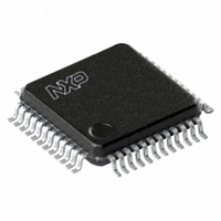
SC68C652BIB48,157 NXP Semiconductors, SC68C652BIB48,157 Datasheet - Page 9

SC68C652BIB48,157
Manufacturer Part Number
SC68C652BIB48,157
Description
IC UART DUAL 48LQFP
Manufacturer
NXP Semiconductors
Datasheet
1.SC68C652BIB48128.pdf
(43 pages)
Specifications of SC68C652BIB48,157
Features
2 Channels
Number Of Channels
2, DUART
Fifo's
32 Byte
Voltage - Supply
2.5V, 3.3V, 5V
With Auto Flow Control
Yes
With Irda Encoder/decoder
Yes
With False Start Bit Detection
Yes
With Modem Control
Yes
Mounting Type
Surface Mount
Package / Case
48-LFQFP
Voltage
2.25 V ~ 5.5 V
Lead Free Status / RoHS Status
Lead free / RoHS Compliant
Other names
935278766157
SC68C652BIB48
SC68C652BIB48
SC68C652BIB48
SC68C652BIB48
Available stocks
Company
Part Number
Manufacturer
Quantity
Price
Company:
Part Number:
SC68C652BIB48,157
Manufacturer:
NXP Semiconductors
Quantity:
10 000
NXP Semiconductors
SC68C652B_2
Product data sheet
6.2 Internal registers
6.3 FIFO operation
The SC68C652B provides two sets of internal registers (A and B) consisting of
17 registers each for monitoring and controlling the functions of each channel of the
UART. These registers are shown in
registers (THR/RHR), interrupt status and control registers (IER/ISR), a FIFO control
register (FCR), line status and control registers (LCR/LSR), modem status and control
registers (MCR/MSR), programmable data rate (clock) control registers (DLL/DLM), and a
user accessible scratchpad register (SPR), along with advanced feature registers EFR
and Xon1, Xon2, Xoff1 and Xoff2.
Table 4.
[1]
[2]
[3]
The 32-byte transmit and receive data FIFOs are enabled by the FIFO Control Register
bit 0 (FCR[0]). With SC68C2550B devices, the user can set the receive trigger level, but
not the transmit trigger level. The SC68C652B provides independent trigger levels for both
receiver and transmitter. To remain compatible with SC68C2550B, the transmit interrupt
trigger level is set to 16 following a reset. It should be noted that the user can set the
transmit trigger levels by writing to the FCR register, but activation will not take place until
EFR[4] is set to a logic 1. The receiver FIFO section includes a time-out function to ensure
data is delivered to the external CPU. An interrupt is generated whenever the Receive
Holding Register (RHR) has not been read following the loading of a character or the
receive trigger level has not been reached.
A2
General register set (THR/RHR, IER/ISR, MCR/MSR, FCR, LSR, SPR)
0
0
0
0
1
1
1
1
Baud rate register set (DLL/DLM)
0
0
Enhanced register set (EFR, Xon1, Xon2, Xoff1, Xoff2)
0
1
1
1
1
These registers are accessible only when LCR[7] is a logic 0.
These registers are accessible only when LCR[7] is a logic 1.
Enhanced Feature Register, Xon1, Xon2, and Xoff1, Xoff2 are accessible only when the LCR is set to ‘BFh’.
A1
0
0
1
1
0
0
1
1
0
0
1
0
0
1
1
Internal registers decoding
A0
0
1
0
1
0
1
0
1
0
1
0
0
1
0
1
Rev. 02 — 2 November 2009
Read mode
Receive Holding Register
Interrupt Enable Register
Interrupt Status Register
Line Control Register
Modem Control Register
Line Status Register
Modem Status Register
Scratchpad Register
LSB of Divisor Latch
MSB of Divisor Latch
Enhanced Feature Register
Xon1 word
Xon2 word
Xoff1 word
Xoff2 word
Dual UART with 32-byte FIFOs and IrDA encoder/decoder
[2]
Table
4. The UART registers function as data holding
[3]
Write mode
Transmit Holding Register
Interrupt Enable Register
FIFO Control Register
Line Control Register
Modem Control Register
n/a
n/a
Scratchpad Register
LSB of Divisor Latch
MSB of Divisor Latch
Enhanced Feature Register
Xon1 word
Xon2 word
Xoff1 word
Xoff2 word
SC68C652B
[1]
© NXP B.V. 2009. All rights reserved.
9 of 43


