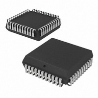
SC16C750IA44,512 NXP Semiconductors, SC16C750IA44,512 Datasheet - Page 14

SC16C750IA44,512
Manufacturer Part Number
SC16C750IA44,512
Description
IC UART 64BYTE 44PLCC
Manufacturer
NXP Semiconductors
Datasheet
1.SC16C750IA44529.pdf
(45 pages)
Specifications of SC16C750IA44,512
Number Of Channels
1, UART
Fifo's
64 Byte
Voltage - Supply
2.5V, 3.3V, 5V
With Auto Flow Control
Yes
With False Start Bit Detection
Yes
With Modem Control
Yes
With Cmos
Yes
Mounting Type
Surface Mount
Package / Case
44-PLCC
Voltage
2.25 V ~ 5.5 V
Transmit Fifo
64Byte
Receive Fifo
64Byte
Transmitter And Receiver Fifo Counter
Yes
Package Type
PLCC
Operating Supply Voltage (max)
5.5V
Mounting
Surface Mount
Pin Count
44
Operating Temperature (min)
-40C
Operating Temperature (max)
85C
Operating Temperature Classification
Industrial
Lead Free Status / RoHS Status
Lead free / RoHS Compliant
Features
-
Lead Free Status / Rohs Status
Compliant
Other names
935270053512
SC16C750IA44
SC16C750IA44
SC16C750IA44
SC16C750IA44
Available stocks
Company
Part Number
Manufacturer
Quantity
Price
Company:
Part Number:
SC16C750IA44,512
Manufacturer:
NXP Semiconductors
Quantity:
10 000
Philips Semiconductors
9397 750 11623
Product data
6.7 Sleep mode
6.8 Loop-back mode
The SC16C750 is designed to operate with low power consumption. A special sleep
mode is included to further reduce power consumption when the chip is not being
used. With IER[4] enabled (set to a logic 1), the SC16C750 enters the sleep mode,
but resumes normal operation when a start bit is detected, a change of state on any
of the modem input pins RX, RI, CTS, DSR, DCD, or a transmit data is provided by
the user. If the sleep mode is enabled and the SC16C750 is awakened by one of the
conditions described above, it will return to the sleep mode automatically after the last
character is transmitted or read by the user. In any case, the sleep mode will not be
entered while an interrupt(s) is pending. The SC16C750 will stay in the sleep mode of
operation until it is disabled by setting IER[4] to a logic 0.
The internal loop-back capability allows on-board diagnostics. In the loop-back mode,
the normal modem interface pins are disconnected and reconfigured for loop-back
internally. MCR[0-3] register bits are used for controlling loop-back diagnostic testing.
In the loop-back mode, OUT1 and OUT2 in the MCR register (bits 2-3) control the
modem RI and DCD inputs, respectively. MCR signals DTR and RTS (bits 0-1) are
used to control the modem CTS and DSR inputs, respectively. The transmitter output
(TX) and the receiver input (RX) are disconnected from their associated interface
pins, and instead are connected together internally (see
DCD, and RI are disconnected from their normal modem control input pins, and
instead are connected internally to DTR, RTS, OUT1 and OUT2. Loop-back test data
is entered into the transmit holding register via the user data bus interface, D0-D7.
The transmit UART serializes the data and passes the serial data to the receive
UART via the internal loop-back connection. The receive UART converts the serial
data back into parallel data that is then made available at the user data interface
D0-D7. The user optionally compares the received data to the initial transmitted data
for verifying error-free operation of the UART TX/RX circuits.
In this mode, the receiver and transmitter interrupts are fully operational. The Modem
Control Interrupts are also operational. However, the interrupts can only be read
using lower four bits of the Modem Status Register (MSR[0-3]) instead of the four
Modem Status Register bits 4-7. The interrupts are still controlled by the IER.
Rev. 04 — 20 June 2003
© Koninklijke Philips Electronics N.V. 2003. All rights reserved.
Figure
UART with 64-byte FIFO
SC16C750
5). The CTS, DSR,
14 of 45


