TDA5211 Infineon Technologies, TDA5211 Datasheet - Page 17
TDA5211
Manufacturer Part Number
TDA5211
Description
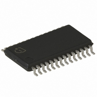
IC FSK/ASK RECEIVER P-TSSOP-28
Manufacturer
Infineon Technologies
Type
Receiverr
Datasheet
1.TDA5211.pdf
(52 pages)
Specifications of TDA5211
Package / Case
28-TSSOP
Frequency
310MHz ~ 350MHz
Sensitivity
-110dBm
Modulation Or Protocol
ASK, FSK
Applications
Alarm Systems, Communication Systems
Current - Receiving
5.7mA
Data Interface
PCB, Surface Mount
Antenna Connector
PCB, Surface Mount
Voltage - Supply
4.5 V ~ 5.5 V
Operating Temperature
-40°C ~ 105°C
Operating Frequency
350 MHz
Operating Supply Voltage
5 V
Maximum Operating Temperature
+ 150 C
Minimum Operating Temperature
- 40 C
Mounting Style
SMD/SMT
Operating Temperature (min)
-40C
Operating Temperature Classification
Automotive
Product Depth (mm)
4.4mm
Product Length (mm)
9.7mm
Operating Supply Voltage (min)
4.5V
Operating Supply Voltage (typ)
5V
Operating Supply Voltage (max)
5.5V
Lead Free Status / RoHS Status
Lead free / RoHS Compliant
Features
-
Memory Size
-
Data Rate - Maximum
-
Lead Free Status / Rohs Status
Compliant
Other names
SP000016390
TDA5211INTR
TDA5211XT
TDA5211XTINTR
TDA5211XTINTR
TDA5211INTR
TDA5211XT
TDA5211XTINTR
TDA5211XTINTR
Available stocks
Company
Part Number
Manufacturer
Quantity
Price

Part Number:
TDA5211
Manufacturer:
INFINEON/英飞凌
Quantity:
20 000
Part Number:
TDA5211B3
Manufacturer:
INFINEON/英飞凌
Quantity:
20 000
Company:
Part Number:
TDA5211B4
Manufacturer:
SIEMENS
Quantity:
5 510
Part Number:
TDA5211B4
Manufacturer:
INFINEON/英飞凌
Quantity:
20 000


Wireless Components
RF
TAGC
DGND
VCC
LNI
14
13
3
4
VCC AGND
3.4.1
LNA
2,7
3.3 Functional Block Diagram
3.4 Functional Blocks
5,10
LNO
VCC
6
Figure 3-2
Low Noise Amplifier (LNA)
The LNA is an on-chip cascode amplifier with a voltage gain of 15 to 20dB. The
gain figure is determined by the external matching networks situated ahead of
LNA and between the LNA output LNO (Pin 6) and the Mixer Inputs MI and MIX
(Pins 8 and 9). The noise figure of the LNA is approximately 3dB, the current
consumption is 500µA. The gain can be reduced by approximately 18dB. The
switching point of this AGC action can be determined externally by applying a
threshold voltage at the THRES pin (Pin 23). This voltage is compared internally
with the received signal (RSSI) level generated by the limiter circuitry. In case
that the RSSI level is higher than the threshold voltage the LNA gain is reduced
and vice versa. The threshold voltage can be generated by attaching a voltage
divider between the 3VOUT pin (Pin 24) which provides a temperature stable
3V output generated from the internal bandgap voltage and the THRES pin as
described in Section 4.1. The time constant of the AGC action can be deter-
MI
: 1 / 2
(FSEL)
8
11
MIX
9
12
IFO
VCO
Loop
Filter
OTA
Filter
IF
Main Block Diagram
LIM
: 128 / 64
CSEL
17
16
LIMX
18
LIMITER
DET
3 - 9
TDA 5211
TDA 5211
PLL Demod
TDA 5211
CRYSTAL
FSK
1
Crystal
OSC
MSEL
28
15
+
+
-
-
FSK
ASK
FFB
22
OPP
21
+
-
OP
Functional Description
U
REF
SLP
Specification, May 2001
19
Reference
Reference
Bandgap
PDWN
AGC
SLN
20
-
+
SLICER
DETECTOR
27
Functional_diagram_5211.wmf
PEAK
TDA 5211
25
24
23
26
DATA
PDO
THRES
3VOUT
Related parts for TDA5211
Image
Part Number
Description
Manufacturer
Datasheet
Request
R

Part Number:
Description:
Manufacturer:
Infineon Technologies AG
Datasheet:
Part Number:
Description:
Manufacturer:
Infineon Technologies AG
Datasheet:
Part Number:
Description:
Manufacturer:
Infineon Technologies AG
Datasheet:
Part Number:
Description:
Manufacturer:
Infineon Technologies AG
Datasheet:
Part Number:
Description:
Manufacturer:
Infineon Technologies AG
Datasheet:
Part Number:
Description:
Manufacturer:
Infineon Technologies AG
Datasheet:
Part Number:
Description:
Manufacturer:
Infineon Technologies AG
Datasheet:
Part Number:
Description:
16-bit microcontroller with 2x2 KByte RAM
Manufacturer:
Infineon Technologies AG
Datasheet:
Part Number:
Description:
NPN silicon RF transistor
Manufacturer:
Infineon Technologies AG
Datasheet:
Part Number:
Description:
NPN silicon RF transistor
Manufacturer:
Infineon Technologies AG
Datasheet:
Part Number:
Description:
NPN silicon RF transistor
Manufacturer:
Infineon Technologies AG
Datasheet:
Part Number:
Description:
NPN silicon RF transistor
Manufacturer:
Infineon Technologies AG
Datasheet:
Part Number:
Description:
Si-MMIC-amplifier in SIEGET 25-technologie
Manufacturer:
Infineon Technologies AG
Datasheet:
Part Number:
Description:
IGBT Power Module
Manufacturer:
Infineon Technologies AG
Datasheet:
Part Number:
Description:
IC for switching-mode power supplies
Manufacturer:
Infineon Technologies AG
Datasheet: