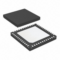
ATA5824-PLQW Atmel, ATA5824-PLQW Datasheet - Page 21

ATA5824-PLQW
Manufacturer Part Number
ATA5824-PLQW
Description
IC TXRX UHF ASK/FSK 48QFN
Manufacturer
Atmel
Datasheet
1.ATA5824-PLQW.pdf
(98 pages)
Specifications of ATA5824-PLQW
Frequency
433 ~ 435MHz; 866 ~ 870MHz
Data Rate - Maximum
20kbps
Modulation Or Protocol
ASK, FSK
Applications
RKE, TPM, Security Systems
Power - Output
10dBm
Sensitivity
-116dBm
Voltage - Supply
2.15 V ~ 3.6 V or 4.4 V ~ 5.25 V
Current - Receiving
10.5mA
Current - Transmitting
10.5mA
Data Interface
PCB, Surface Mount
Antenna Connector
PCB, Surface Mount
Operating Temperature
-40°C ~ 105°C
Package / Case
48-VQFN Exposed Pad, 48-HVQFN, 48-SQFN, 48-DHVQFN
Lead Free Status / RoHS Status
Lead free / RoHS Compliant
Memory Size
-
Available stocks
Company
Part Number
Manufacturer
Quantity
Price
Company:
Part Number:
ATA5824-PLQW
Manufacturer:
ATMEL
Quantity:
3 500
Part Number:
ATA5824-PLQW
Manufacturer:
ATMEL/爱特梅尔
Quantity:
20 000
7.13
4829D–RKE–06/06
Output Power Setting and PA Matching at RF_OUT
The Power Amplifier (PA) is a single-ended open collector stage which delivers a current pulse
which is nearly independent of supply voltage, temperature and tolerances due to band-gap sta-
bilization. Resistor R
current in the PA. A higher resistor value results in a lower reference current, a lower output
power and a lower current consumption of the PA. The usable range of R
PWR_H pin switches the output power range between about 0 dBm to 5 dBm (PWR_H = GND)
and 5 dBm to 10 dBm (PWR_H = AVCC) by multiplying this reference current with a factor 1
(PWR_H = GND) and 2.5 (PWR_H = AVCC) which corresponds to about 5 dB more output
power.
If the PA is switched off in TX mode, the current consumption without output stage and with
V
433.92 MHz.
The maximum output power is achieved with optimum load resistances R
7-7 on page
achieved by absorbing it into the matching network, consisting of L
7-12 on page
of the power amplifier's last stage. The matching of the PA output was done with the circuit
according to
these elements may be necessary to compensate individual board layout parasitics.
Example:
According to
11 dBm, the overall current consumption is typically 17.8 mA. Hence the PA needs
17.8 mA - 6.95 mA = 10.85 mA in this mode which corresponds to an overall power amplifier
efficiency of the PA of (10
Using a higher resistor in this example of R1 = 1.091
rent in the PA of 10.85 mA/1.091 = 9.95 mA and 10
using a new load resistance of 300
11 dBm
6.95 mA + 9.95 mA = 16.9 mA.
The values of
quality factors Q according to
Looking to the 433.92 MHz/11 dBm case with the quality factor of Q
t o r L
R
0.32 dB losses in this inductor. Taking this into account the PA efficiency is then 42% instead of
38.6%.
Be aware that the high power mode (PWR_H = AVCC) can only be used with a supply voltage
higher than 2.7V, whereas the low power mode (PWR_H = GND) can be used down to 2.15V as
can be seen in the section
The supply blocking capacitor C
matching network because of the RF current flowing through it.
S1
loss
= V
= 2
1
S2
–
i s e s t i m a t e d w i t h t h e p a r a l l e l e q u i v a l e n t r e s i s t a n c e o f t h e i n d u c t o r
0.38 dB = 10.6 dBm and the overall current consumption is
= 3V, T
22. The compensation of the 1.0 pF output capacitance of the RF_OUT pin will be
Figure 7-12 on page 22
22. There must be also a low resistive DC path to AVCC to deliver the DC current
Table 7-7 on page 22
Table 7-7 on page
f
amb
L1
1
= 25°C is typically 6.5 mA for 868.3 MHz and 6.95 mA for 315 MHz and
(see
Q
(11dBm/10)
L1
“Electrical Characteristics: General” on page
Figure 7-12 on page
and the matching loss with 10 log (1 + R
Table 7-7 on page
2
(10 nF) in
22, with a frequency of 433.92 MHz and output power of
were measured with standard multi-layer chip inductors with
1 mW)/(3V
with the values in
1.091 = 327 . The resulting output power is then
Figure 7-12 on page 22
22) sets a reference current which controls the
22.
10.85 mA)
log(1.091) = 0.38 dB less output power if
22 k = 24 k results in 9.1% less cur-
Table
ATA5823/ATA5824
7-7. Note that value changes of
100% = 38.6% in this case.
1
L1
has to be placed close to the
, C
Lopt
= 43 the loss in this induc-
1
, C
72.
/R
1
Lopt
is 15 k to 56 k . The
loss
3
as shown in
according to
) which is equal to
Figure
Table
21


