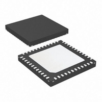
ATA5824-PLQW Atmel, ATA5824-PLQW Datasheet - Page 64

ATA5824-PLQW
Manufacturer Part Number
ATA5824-PLQW
Description
IC TXRX UHF ASK/FSK 48QFN
Manufacturer
Atmel
Datasheet
1.ATA5824-PLQW.pdf
(98 pages)
Specifications of ATA5824-PLQW
Frequency
433 ~ 435MHz; 866 ~ 870MHz
Data Rate - Maximum
20kbps
Modulation Or Protocol
ASK, FSK
Applications
RKE, TPM, Security Systems
Power - Output
10dBm
Sensitivity
-116dBm
Voltage - Supply
2.15 V ~ 3.6 V or 4.4 V ~ 5.25 V
Current - Receiving
10.5mA
Current - Transmitting
10.5mA
Data Interface
PCB, Surface Mount
Antenna Connector
PCB, Surface Mount
Operating Temperature
-40°C ~ 105°C
Package / Case
48-VQFN Exposed Pad, 48-HVQFN, 48-SQFN, 48-DHVQFN
Lead Free Status / RoHS Status
Lead free / RoHS Compliant
Memory Size
-
Available stocks
Company
Part Number
Manufacturer
Quantity
Price
Company:
Part Number:
ATA5824-PLQW
Manufacturer:
ATMEL
Quantity:
3 500
Part Number:
ATA5824-PLQW
Manufacturer:
ATMEL/爱特梅尔
Quantity:
20 000
Table 14-5.
14.3
64
Mode
TX
Full-duplex Operation
ATA5823/ATA5824
TX Modulation Schemes
ASK/_NFSK
0
1
The transceiver is set to full-duplex mode (FD mode) by using the bits OPM0, OPM1 and OPM2
in the control register 1. In FD mode 2 transceiver exchange the content of the TX buffer simul-
taneously. One transceiver must be configured as master and one as slave.
Table 14-6.
Before activating FD mode in both transceivers, the bit rate must be selected in control register 6
(Baud1 = 0, Baud0 = 1). Additionally, in the slave the limits for the Bit-check and the number of
bits to be checked during the Bit-check N
(Lim_min0 ... Lim_min5, Lim_max0 ... Lim_max5, BitChk0, BitChk1).
After activating the FD mode in control register 1, both transceivers are in the startup mode. Dur-
ing the startup mode, in master and slave, the TX data stream can be written in the TX buffer.
In the master the TX data stream consists of preburst, startbit, synchronization pattern (3 bytes)
and maximally 8 bytes of data. The preburst contains a sequence of “11111...”. The minimum
applicable preburst length is 15 bits and can be extended in 8 bit steps up to 95 bits. The value
of the start bit is fixed and must be a 0. The position of the start bit is the LSB in the last byte of
the preburst. The synchronization pattern contains 3 bytes with a fixed value (Byte1: FF hex,
Byte2: 00 hex, Byte3: 00 hex). The data block is user defined and contains maximally 8 bytes. If
the preburst contains more than 39 bits the area for the data block will be equally reduced
ure 14-12 on page
In the slave the TX data stream consists of the synchronization pattern (3 bytes) and also maxi-
mally 8 bytes of data. The synchronization pattern contains 3 bytes with a fixed value (Byte1:
00 hex, Byte2: 7F hex, Byte3: FF hex). The data block is user defined and contains maximally
8 bytes
slave.
OPM2
(Figure 14-12 on page
P_Mode
1
1
X
X
X
X
0
0
1
1
0
0
1
1
Control Register 1
65.)
T_Mode
OPM1
0
0
0
0
1
1
0
0
0
0
1
1
0
1
65). The length of the data block must be equal in the master and
Bit in TX/RX
Data Buffer
Bit-check
X
X
X
X
1
0
1
0
1
0
1
0
OPM0
1
1
must be adjusted in control register 5 and 6
Level on Pin
SDI_TMDI
X
X
X
X
X
X
X
X
1
0
1
0
Full-duplex mode (Master)
Full-duplex mode (Slave)
Function
f
f
ASK
ASK
f
f
FSK_L
FSK_H
off
on
f
f
f
f
RF
f
f
ASK
ASK
ASK
ASK
f
f
FSK_H
FSK_H
FSK_L
FSK_L
4829D–RKE–06/06
OUT
on
off
on
off
f
f
f
f
FSK_H
ASK
ASK
FSK_L
on
off
(Fig-


