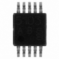
TDA7116F Infineon Technologies, TDA7116F Datasheet - Page 24

TDA7116F
Manufacturer Part Number
TDA7116F
Description
IC TX ASK/FSK 868MHZ 10-TSSOP
Manufacturer
Infineon Technologies
Datasheet
1.TDA7116F.pdf
(36 pages)
Specifications of TDA7116F
Frequency
866MHz ~ 870MHz
Modulation Or Protocol
ASK, FSK
Power - Output
13dBm
Current - Transmitting
14.2mA
Data Interface
PCB, Surface Mount
Antenna Connector
PCB, Surface Mount
Voltage - Supply
2.1 V ~ 4 V
Operating Temperature
-40°C ~ 85°C
Package / Case
10-TSSOP
Lead Free Status / RoHS Status
Lead free / RoHS Compliant
Features
-
Applications
-
Memory Size
-
Data Rate - Maximum
-
Lead Free Status / RoHS Status
Lead free / RoHS Compliant, Lead free / RoHS Compliant
Other names
SP000611114
Available stocks
Company
Part Number
Manufacturer
Quantity
Price
Company:
Part Number:
TDA7116FHTMA1
Manufacturer:
TI
Quantity:
12 000
If the FSK switch is closed, Cv
FSK switch is open, Cv2 (C2 in the application diagram) can be calculated.
Csw:
Remark:
on the parasitic and thus on the layout also and must be adapted for the specific
application board.
3.5
The CLKOUT pin is an open collector output. An external pull up resistor (RL) should be
connected between this pin and the positive supply voltage. The value of RL is
depending on the clock frequency and the load capacitance CLD (PCB board plus input
capacitance of the microcontroller). RL can be calculated to:
Table 7
Remark:
Data Sheet
parallel capacitance of the FSK switch (3 pF incl. layout parasitics)
These calculations are only approximations. The necessary values depend
Design Hints on the Clock Output (CLKOUT)
Clock Output
To achieve a low current consumption and a low
spurious radiation, the largest possible RL should be chosen.
CL
10
20
[
5
pF
Cv
]
2
=
C
2
RL
±
=
Cv
fCLKOUT=847.5 kHz
is equal to Cv1 (C1 in the application diagram). If the
=
Csw
±
fCLKOUT
=
∗
Cv
CL
1
24
1
±
(
−
Cv
1
1
(
+
Cv
*
+
ω
8
)
+
2
−
*
)
L
CLD
Cv
∗
(
Cv
1
1
RL
+
Csw
[
kOhm
6.8
27
12
)
]
V 1.0, 2009-03-05
Applications
TDA7116F


