FSB50250UD Fairchild Semiconductor, FSB50250UD Datasheet
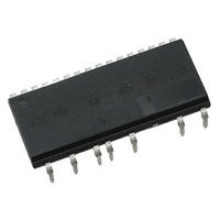
MOD SPM 500V 0.5A SPM23-HD

FSB50250UD

Manufacturer Part Number
FSB50250UD
Description
MOD SPM 500V 0.5A SPM23-HD
Manufacturer
Fairchild Semiconductor
Series
SPM™r
Type
FETr
Datasheet

Specifications of FSB50250UD

Configuration
3 Phase
Current
1.1A
Voltage
500V
Voltage - Isolation
1500Vrms
Package / Case
SPM23HD
Lead Free Status / RoHS Status
Lead free / RoHS Compliant
©2010 Fairchild Semiconductor Corporation
FSB50250UD Rev. A
FSB50250UD
Smart Power Module (SPM
Features
• 500V R
• 3 divided negative dc-link terminals for inverter current sens-
• HVIC for gate driving and undervoltage protection
• 3/5V CMOS/TTL compatible, active-high interface
• Optimized for low electromagnetic interference
• Isolation voltage rating of 1500Vrms for 1min.
• Embedded bootstrap diode in the package
Absolute Maximum Ratings
Symbol
high voltage integrated circuit (HVIC)
ing applications
T
R
V
V
V
I
I
V
I
V
P
D25
D80
T
STG
DP
qJC
ISO
PN
CC
BS
IN
D
J
DS(on)
DC Link Input Voltage,
Drain-source Voltage of each FRFET
Each FRFET Drain Current, Continuous
Each FRFET Drain Current, Peak
Maximum Power Dissipation
Control Supply Voltage
High-side Bias Voltage
Input Signal Voltage
Operating Junction Temperature
Storage Temperature
Junction to Case Thermal Resistance
Isolation Voltage
=4.2W(max) 3-phase FRFET inverter including
Parameter
®
)
T
T
T
T
Applied between V
Applied between V
Applied between IN and COM
Each FRFET under inverter operating con-
dition (Note 1)
60Hz, Sinusoidal, 1 minute, Connection
pins to heatsink
C
C
C
C
= 25°C
= 80°C
= 25°C, PW < 100ms
= 25°C, Each FRFET
1
General Description
FSB50250UD is a tiny smart power module (SPM
FRFET technology as a compact inverter solution for small
power motor drive applications such as fan motors and water
suppliers. It is composed of 6 fast-recovery MOSFET (FRFET),
and
FSB50250UTD provides low electromagnetic interference (EMI)
characteristics with optimized switching speed. Moreover, since
it employs FRFET as a power switch, it has much better
ruggedness and larger safe operation area (SOA) than that of
an IGBT-based power module or one-chip solution. The
package is optimized for the thermal performance and
compactness for the use in the built-in motor application and
any other application where the assembly space is concerned.
FSB50250UD is the most solution for the compact inverter
providing the energy efficiency, compactness, and low
electromagnetic interference.
Conditions
3
CC
B(U)
and COM
half-bridge
-U, V
B(V)
-V, V
Motion-SPM
HVICs
B(W)
-W
for
-0.3 ~ VCC+0.3
-40 ~ 150
-40 ~ 125
Rating
FRFET
1500
500
1.1
0.8
2.8
9.3
13
20
20
www.fairchildsemi.com
gate
®
April 2010
) based on
Units
°C/W
V
driving.
°C
°C
W
V
A
A
A
V
V
V
rms
TM

Related parts for FSB50250UD

FSB50250UD Summary of contents

Page 1

... FSB50250UD is the most solution for the compact inverter providing the energy efficiency, compactness, and low electromagnetic interference. ...

Page 2

... Note: Source terminal of each low-side MOSFET is not connected to supply ground or bias voltage ground inside SPM ure 2 and 5. Figure 1. Pin Configuration and Internal Block Diagram (Bottom View) FSB50250UD Rev. A Pin Description IC Common Supply Ground Bias Voltage for U Phase High Side FRFET Driving ...

Page 3

... Please see Figure 5 for the switching time definition with the switching test circuit of Figure 6. 4. The peak current and voltage of each FRFET during the switching operation should be included in the safe operating area (SOA). Please see Figure 6 for the RBSOA test cir- cuit that is same as the switching test circuit. FSB50250UD Rev 25°C, V ...

Page 4

... Note: Built in bootstrap diode includes around 15 Ω resistance characteristic. Figure 2. Built in Bootstrap Diode Characteristics Package Marking & Ordering Information Device Marking Device FSB50250UD FSB50250UD FSB50250UD Rev. A Conditions I = 0.1A 25° 0.1A 25° Built in Bootstrap Diode V -I Characteristic ...

Page 5

... Figure 3. Recommended CPU Interface and Bootstrap Circuit with Parameters 3.80 3.80 Note: Attach the thermocouple on top of the heatsink-side of SPM FSB50250UD Rev. A Conditions Applied between P and N Applied between V and COM CC Applied between V and output( ...

Page 6

... V IN 100 (a) Turn- Figure 6. Switching and RBSOA(Single-pulse) Test Circuit (Low-side) Input Signal UV Protection Status Low-side Supply, V MOSFET Current Input Signal UV Protection Status High-side Supply, V MOSFET Current FSB50250UD Rev 120 Figure 5. Switching Time Definition R EH VCC VB HIN HO LIN VS COM LO C One-leg Diagram of SPM ...

Page 7

... 15-V Supply FSB50250UD Rev (1) COM (2) V B(U) (3) V CC(U) VCC VB (4) IN (UH) HIN HO (5) IN (UL) LIN VS C COM LO 1 (6) V S(U) (7) V B(V) (8) V CC(V) VCC VB (9) IN (VH) HIN HO (10) IN (VL) LIN VS C COM LO 1 (11) V S(V) (12) V B(W) (13) V CC(W) ...

Page 8

... Detailed Package Outline Drawings #1 (1.165) 15*1.778=26.67 13.34 #1 #17 12.23 (2.275) #17 #19 (0.30) 0.60 ±0.05 #17,18,21,22,23 LEAD Max 1.00 FSB50250UD Rev. A 16-Max 1.00 16-0.50 ±0.05 13-(0.30) #16 ±0.30 13.34 #16 #23 13.13 29.00 ±0.20 2x3.90=7.80 ±0.30 4x3.90=15.60 ±0.30 1.95 ±0.30 #23 (0.30) 0.50 ±0.05 #19, 20 LEAD Max 1 ...

Page 9

... FSB50250UD Rev Rev. I15 www.fairchildsemi.com ...

Related keywords