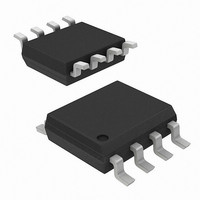
FDS4435BZ_F085 Fairchild Semiconductor, FDS4435BZ_F085 Datasheet - Page 2

FDS4435BZ_F085
Manufacturer Part Number
FDS4435BZ_F085
Description
MOSFET P-CH 30V 8-SOIC
Manufacturer
Fairchild Semiconductor
Series
PowerTrench®r
Datasheet
1.FDS4435BZ_F085.pdf
(6 pages)
Specifications of FDS4435BZ_F085
Fet Type
MOSFET P-Channel, Metal Oxide
Fet Feature
Logic Level Gate
Rds On (max) @ Id, Vgs
20 mOhm @ 8.8A, 10V
Drain To Source Voltage (vdss)
30V
Current - Continuous Drain (id) @ 25° C
8.8A
Vgs(th) (max) @ Id
3V @ 250µA
Gate Charge (qg) @ Vgs
40nC @ 10V
Input Capacitance (ciss) @ Vds
1845pF @ 15V
Power - Max
1W
Mounting Type
Surface Mount
Package / Case
8-SOIC (0.154", 3.90mm Width)
Configuration
Single
Transistor Polarity
P-Channel
Resistance Drain-source Rds (on)
26 mOhms
Forward Transconductance Gfs (max / Min)
24 S
Drain-source Breakdown Voltage
- 30 V
Gate-source Breakdown Voltage
+/- 25 V
Continuous Drain Current
- 8.8 A
Power Dissipation
2.5 W
Maximum Operating Temperature
+ 150 C
Mounting Style
SMD/SMT
Minimum Operating Temperature
- 55 C
Lead Free Status / RoHS Status
Lead free / RoHS Compliant
©2009 Fairchild Semiconductor Corporation
FDS4435BZ_F085 Rev.A
Electrical Characteristics
Off Characteristics
On Characteristics
Dynamic Characteristics
Switching Characteristics
Drain-Source Diode Characteristics
NOTES:
1. R
2. Pulse Test: Pulse Width < 300Ps, Duty cycle < 2.0%.
3. The diode connected between the gate and source serves only as protection against ESD. No gate overvoltage rating is implied.
4. Starting T
BV
'BV
I
I
V
r
g
C
C
C
R
t
t
t
t
Q
Q
Q
Q
V
t
Q
'V
DSS
GSS
d(on)
r
d(off)
f
rr
DS(on)
FS
GS(th)
SD
the user's board design.
iss
oss
rss
g
'T
'T
g
g
gs
gd
rr
Symbol
TJA
DSS
GS(th)
DSS
J
J
is determined with the device mounted on a 1in
J
= 25°C, L = 1mH, I
Drain to Source Breakdown Voltage
Breakdown Voltage Temperature
Coefficient
Zero Gate Voltage Drain Current
Gate to Source Leakage Current
Gate to Source Threshold Voltage
Gate to Source Threshold Voltage
Temperature Coefficient
Static Drain to Source On Resistance
Forward Transconductance
Input Capacitance
Output Capacitance
Reverse Transfer Capacitance
Gate Resistance
Turn-On Delay Time
Rise Time
Turn-Off Delay Time
Fall Time
Total Gate Charge
Total Gate Charge
Gate to Source Charge
Gate to Drain “Miller” Charge
Source to Drain Diode Forward Voltage
Reverse Recovery Time
Reverse Recovery Charge
AS
= -7A, V
a. 50°C/W when mounted on
a 1 in
Parameter
DD
2
pad of 2 oz copper.
= -30V, V
2
T
pad 2 oz copper pad on a 1.5 x 1.5 in. board of FR-4 material. R
J
GS
= 25°C unless otherwise noted
= -10V
V
V
V
V
V
f = 1MHz
f = 1MHz
V
I
V
V
V
V
V
I
I
I
V
V
D
F
D
D
DD
GS
GS
GS
GS
GS
GS
GS
DS
DS
GS
DS
GS
= -8.8A, di/dt = 100A/Ps
= -250PA, referenced to 25°C
= -250PA, V
= -250PA, referenced to 25°C
= 0V to -10V
= 0V to -5V
= -15V, V
= -15V, I
= -10V, R
= -5V, I
= 0V, I
= -24V, V
= V
= -10V, I
= -4.5V, I
= -10V, I
= ±25V, V
2
DS
Test Conditions
, I
S
D
D
= -8.8A
D
D
D
GS
GEN
= -8.8A
GS
= -8.8A,
DS
D
= -250PA
GS
= -8.8A, T
= -8.8A
= -6.7A
= 0V,
= 0V
= 0V
= 6:
= 0V
V
I
D
DD
= -8.8A
(Note 2)
= -15V,
J
= 125°C
b. 125°C/W when mounted on
TJC
a minimum pad of 2 oz copper.
is guaranteed by design while R
Min
-30
-1
1385
-0.9
Typ
-2.1
-21
275
230
5.2
7.4
4.5
29
23
16
26
22
24
10
30
12
28
16
6
6
1845
Max
-1.2
±10
365
345
20
35
28
20
12
48
22
40
23
44
35
TCA
-3
www.fairchildsemi.com
1
is determined by
mV/°C
mV/°C
Units
m:
PA
PA
nC
nC
nC
nC
nC
pF
pF
pF
ns
ns
ns
ns
ns
V
:
V
S
V


