FCH35N60 Fairchild Semiconductor, FCH35N60 Datasheet - Page 2
FCH35N60
Manufacturer Part Number
FCH35N60
Description
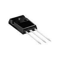
MOSFET N-CH 600V 35A TO-247
Manufacturer
Fairchild Semiconductor
Series
SuperMOS™r
Datasheet
1.FCH35N60.pdf
(8 pages)
Specifications of FCH35N60
Fet Type
MOSFET N-Channel, Metal Oxide
Fet Feature
Standard
Rds On (max) @ Id, Vgs
98 mOhm @ 17.5A, 10V
Drain To Source Voltage (vdss)
600V
Current - Continuous Drain (id) @ 25° C
35A
Vgs(th) (max) @ Id
5V @ 250µA
Gate Charge (qg) @ Vgs
181nC @ 10V
Input Capacitance (ciss) @ Vds
6640pF @ 25V
Power - Max
312.5W
Mounting Type
Through Hole
Package / Case
TO-247-3
Transistor Polarity
N-Channel
Resistance Drain-source Rds (on)
79 mOhms
Drain-source Breakdown Voltage
600 V
Gate-source Breakdown Voltage
30 V
Continuous Drain Current
35 A
Power Dissipation
312.5 W
Forward Transconductance Gfs (max / Min)
28.8 S
Gate Charge Qg
139 nC
Mounting Style
Through Hole
Lead Free Status / RoHS Status
Lead free / RoHS Compliant
Available stocks
Company
Part Number
Manufacturer
Quantity
Price

Part Number:
FCH35N60
Manufacturer:
FAIRCHILD/仙童
Quantity:
20 000


FCH35N60 Rev. A1
Notes:
1: Repetitive Rating: Pulse width limited by maximum junction temperature
2: I
3: I
4: Essentially Independent of Operating Temperature Typical Characteristics
Package Marking and Ordering Information
Electrical Characteristics
Off Characteristics
On Characteristics
Dynamic Characteristics
Switching Characteristics
Drain-Source Diode Characteristics
BV
ΔBV
/
BV
I
I
V
R
g
C
C
C
C
C
Q
Q
Q
ESR
t
t
t
t
I
I
V
t
Q
DSS
GSS
d(on)
r
d(off)
f
S
SM
rr
FS
GS(th)
SD
DS(on)
iss
oss
rss
oss
oss
g
gs
gd
rr
AS
SD
Device Marking
DSS
DS
Symbol
ΔT
= 17.5A, V
DSS
≤ 35A, di/dt ≤ 200A/μs, V
eff.
FCH35N60
J
DD
= 50V, R
Maximum Continuous Drain to Source Diode Forward Current
Maximum Pulsed Drain to Source Diode Forward Current
Drain to Source Diode Forward Voltage
Reverse Recovery Time
Reverse Recovery Charge
Turn-On Delay Time
Turn-On Rise Time
Turn-Off Delay Time
Turn-Off Fall Time
Input Capacitance
Output Capacitance
Reverse Transfer Capacitance
Output Capacitance
Effective Output Capacitance
Total Gate Charge at 10V
Gate to Source Gate Charge
Gate to Drain “Miller” Charge
Equivalent Series Resistance (G-S)
Drain to Source Breakdown Voltage
Breakdown Voltage Temperature
Coefficient
Drain-Source Avalanche Breakdown
Voltage
Zero Gate Voltage Drain Current
Gate to Body Leakage Current
Gate Threshold Voltage
Static Drain to Source On Resistance
Forward Transconductance
G
= 25Ω, Starting T
DD
≤ BV
FCH35N60
DSS
Device
Parameter
, Starting T
J
= 25°C
J
= 25°C
Package
TO-247
I
I
I
V
V
V
V
V
V
dI
V
V
V
V
f = 1MHz
V
V
V
V
Drain Open, F= 1MHZ
V
R
D
D
D
GS
DS
DS
GS
DD
GS
GS
GS
GS
DS
DS
DS
DS
DS
GS
G
F
= 250μA, V
= 250μA, V
= 250μA, Referenced to 25
/dt = 100A/μs
= 4.7Ω
= 600V, V
= 480V, T
= 0V, I
= 0V, I
= ±30V, V
= 40V, I
= 25V, V
= 480V, V
= 0V to 480V, V
= 480V, I
= 300V, I
= 0V, I
= V
= 10V, I
= 10V
DS
T
Test Conditions
, I
C
SD
2
D
SD
D
Reel Size
D
= 25
D
= 16A
GS
GS
GS
D
D
= 35A
= 17.5A
= 35A
GS
C
= 17.5A
DS
= 250μA
GS
= 35A
= 35A
= 125
= 0V
= 0V, T
= 0V, T
o
-
= 0V
= 0V
= 0V, f = 1.0MHz
C unless otherwise noted
GS
o
C
= 0V
J
J
= 25
= 150
o
(Note 4)
(Note 4)
o
C
C
o
C
Tape Width
-
Min.
600
3.0
-
-
-
-
-
-
-
-
-
-
-
-
-
-
-
-
-
-
-
-
-
-
-
-
-
-
0.079
4990
2380
Typ.
16.3
28.8
120
105
614
650
700
140
113
340
139
0.6
1.4
34
73
31
69
-
-
-
-
-
-
-
-
Quantity
www.fairchildsemi.com
Max.
0.098
±100
6640
3170
250
220
155
181
105
1.4
5.0
78
10
35
1
30
-
-
-
-
-
-
-
-
-
-
-
-
-
Units
V/
nC
nC
nC
μA
pF
pF
pF
pF
pF
nA
ns
ns
ns
ns
ns
μC
Ω
V
V
V
Ω
A
A
V
V
S
o
C
Related parts for FCH35N60
Image
Part Number
Description
Manufacturer
Datasheet
Request
R

Part Number:
Description:
Fairchild Semiconductor [IGBT MODULE]
Manufacturer:
Fairchild Semiconductor
Datasheet:

Part Number:
Description:
Discrete Semiconductor Modules
Manufacturer:
Fairchild Semiconductor
Part Number:
Description:
Discrete Semiconductor Modules
Manufacturer:
Fairchild Semiconductor
Part Number:
Description:
This N-Channel MOSFET is produced using Fairchild Semiconductor’s advanced Power Trench® process
Manufacturer:
Fairchild Semiconductor
Datasheet:
Part Number:
Description:
This N-Channel MOSFET is produced using Fairchild Semiconductor’s advanced Power Trench® process
Manufacturer:
Fairchild Semiconductor
Datasheet:
Part Number:
Description:
This N-Channel MOSFET is produced using Fairchild Semiconductor’s advanced PowerTrench® process
Manufacturer:
Fairchild Semiconductor
Datasheet:
Part Number:
Description:
This N-Channel MOSFET is produced using Fairchild Semiconductor’s advanced PowerTrench® process
Manufacturer:
Fairchild Semiconductor
Datasheet:
Part Number:
Description:
This N-Channel MOSFET is produced using Fairchild Semiconductor’s advanced Power Trench® process
Manufacturer:
Fairchild Semiconductor
Datasheet:
Part Number:
Description:
This N-Channel logic Level MOSFETs are produced using Fairchild Semiconductor‘s advanced Power Trench® process that has been special tailored to minimize the on-state resistance and yet maintain superior switching performance
Manufacturer:
Fairchild Semiconductor
Datasheet:
Part Number:
Description:
This N-Channel MOSFET is produced using Fairchild Semiconductor’s advanced Power Trench® process
Manufacturer:
Fairchild Semiconductor
Datasheet:
Part Number:
Description:
This N-Channel SyncFET™ is produced using Fairchild Semiconductor’s advanced PowerTrench® process
Manufacturer:
Fairchild Semiconductor
Datasheet:
Part Number:
Description:
This N-Channel SyncFET™ is produced using Fairchild Semiconductor’s advanced PowerTrench® process
Manufacturer:
Fairchild Semiconductor
Datasheet:
Part Number:
Description:
This N-Channel SyncFET™ is produced using Fairchild Semiconductor’s advanced PowerTrench® process
Manufacturer:
Fairchild Semiconductor
Datasheet:
Part Number:
Description:
This N-Channel logic Level MOSFETs are produced using Fairchild Semiconductor‘s advanced Power Trench® process that has been special tailored to minimize the on-state resistance and yet maintain superior switching performance
Manufacturer:
Fairchild Semiconductor
Datasheet:
Part Number:
Description:
This N-Channel MOSFET is produced using Fairchild Semiconductor’s advanced Power Trench® process that has been especially tailored to minimize the on-state resistance and yet maintain superior switching performance
Manufacturer:
Fairchild Semiconductor
Datasheet: