AT91SAM7SE256B-AUR Atmel, AT91SAM7SE256B-AUR Datasheet - Page 211
AT91SAM7SE256B-AUR
Manufacturer Part Number
AT91SAM7SE256B-AUR
Description
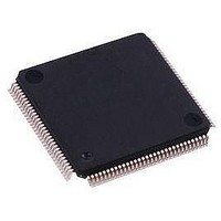
IC ARM7 MCU FLASH 256K 128-LQFP
Manufacturer
Atmel
Series
AT91SAMr
Datasheet
1.AT91SAM7SE256-AU.pdf
(673 pages)
Specifications of AT91SAM7SE256B-AUR
Core Processor
ARM7
Core Size
16/32-Bit
Speed
55MHz
Connectivity
EBI/EMI, I²C, SPI, SSC, UART/USART, USB
Peripherals
Brown-out Detect/Reset, POR, PWM, WDT
Number Of I /o
88
Program Memory Size
256KB (256K x 8)
Program Memory Type
FLASH
Ram Size
32K x 8
Voltage - Supply (vcc/vdd)
1.65 V ~ 1.95 V
Data Converters
A/D 8x10b
Oscillator Type
Internal
Operating Temperature
-40°C ~ 85°C
Package / Case
*
Processor Series
SAM7SE256
Core
ARM7TDMI
Data Bus Width
32 bit
Data Ram Size
32 KB
Interface Type
SPI, USB
Maximum Clock Frequency
48 MHz
Number Of Programmable I/os
88
Maximum Operating Temperature
+ 85 C
Mounting Style
SMD/SMT
Operating Temperature Range
- 40 C to + 85 C
Processor To Be Evaluated
AT91SAM7SE256B
Supply Current (max)
60 uA
Lead Free Status / RoHS Status
Lead free / RoHS Compliant
Eeprom Size
-
Lead Free Status / Rohs Status
Details
Available stocks
Company
Part Number
Manufacturer
Quantity
Price


23.7.1
Name:
Access:
Reset Value:
• MODE: SDRAMC Command Mode
This field defines the command issued by the SDRAM Controller when the SDRAM device is accessed.
• DBW: Data Bus Width
0: Data bus width is 32 bits.
1: Data bus width is 16 bits.
6222F–ATARM–14-Jan-11
0
0
0
0
0
31
23
15
–
–
–
7
–
0
0
0
0
1
MODE
SDRAMC Mode Register
0
0
1
1
0
0
1
0
1
0
30
22
14
SDRAMC_MR
Read/Write
0x00000010
–
–
–
6
–
Description
Normal mode. Any access to the SDRAM is decoded normally.
The SDRAM Controller issues a NOP command when the SDRAM device is accessed regardless of the
cycle.
The SDRAM Controller issues an “All Banks Precharge” command when the SDRAM device is accessed
regardless of the cycle.
The SDRAM Controller issues a “Load Mode Register” command when the SDRAM device is accessed
regardless of the cycle. The address offset with respect to the SDRAM device base address is used to
program the Mode Register. For instance, when this mode is activated, an access to the “SDRAM_Base +
offset” address generates a “Load Mode Register” command with the value “offset” written to the SDRAM
device Mode Register.
The SDRAM Controller issues a “Refresh” Command when the SDRAM device is accessed regardless of
the cycle. Previously, an “All Banks Precharge” command must be issued.
29
21
13
–
–
–
5
–
DBW
28
20
12
–
–
–
4
SAM7SE512/256/32 Preliminary
27
19
11
–
–
–
3
26
18
10
–
–
–
2
MODE
25
17
–
–
9
–
1
24
16
–
–
8
–
0
211
Related parts for AT91SAM7SE256B-AUR
Image
Part Number
Description
Manufacturer
Datasheet
Request
R

Part Number:
Description:
EVAL BOARD FOR AT91SAM7SE
Manufacturer:
Atmel
Datasheet:

Part Number:
Description:
DEV KIT FOR AVR/AVR32
Manufacturer:
Atmel
Datasheet:

Part Number:
Description:
INTERVAL AND WIPE/WASH WIPER CONTROL IC WITH DELAY
Manufacturer:
ATMEL Corporation
Datasheet:
Part Number:
Description:
Low-Voltage Voice-Switched IC for Hands-Free Operation
Manufacturer:
ATMEL Corporation
Datasheet:
Part Number:
Description:
MONOLITHIC INTEGRATED FEATUREPHONE CIRCUIT
Manufacturer:
ATMEL Corporation
Datasheet:
Part Number:
Description:
AM-FM Receiver IC U4255BM-M
Manufacturer:
ATMEL Corporation
Datasheet:
Part Number:
Description:
Monolithic Integrated Feature Phone Circuit
Manufacturer:
ATMEL Corporation
Datasheet:
Part Number:
Description:
Multistandard Video-IF and Quasi Parallel Sound Processing
Manufacturer:
ATMEL Corporation
Datasheet:
Part Number:
Description:
High-performance EE PLD
Manufacturer:
ATMEL Corporation
Datasheet:
Part Number:
Description:
8-bit Flash Microcontroller
Manufacturer:
ATMEL Corporation
Datasheet:
Part Number:
Description:
2-Wire Serial EEPROM
Manufacturer:
ATMEL Corporation
Datasheet: