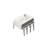
HCPL3700 Fairchild Semiconductor, HCPL3700 Datasheet - Page 4

HCPL3700
Manufacturer Part Number
HCPL3700
Description
Logic Output Optocouplers AC/DC To Logic Interface
Manufacturer
Fairchild Semiconductor
Datasheet
1.HCPL3700.pdf
(11 pages)
Specifications of HCPL3700
Fall Time
400 ns
Logic Gate Type
Darlington Configuration
Rise Time
400 ns
Configuration
1 Channel
Isolation Voltage
2500 Vrms
Output Type
Open Collector
Maximum Propagation Delay Time
40000 ns
Maximum Forward Diode Voltage
0.65 V
Maximum Forward Diode Current
4.4 mA
Maximum Continuous Output Current
30 mA
Maximum Power Dissipation
210 mW
Maximum Operating Temperature
+ 70 C
Minimum Operating Temperature
0 C
Package / Case
DIP-8
Lead Free Status / RoHS Status
Lead free / RoHS Compliant
Other names
HCPL3700_NL
Available stocks
Company
Part Number
Manufacturer
Quantity
Price
Company:
Part Number:
HCPL3700
Manufacturer:
AGILENT
Quantity:
20 000
Part Number:
HCPL3700
Manufacturer:
QTC
Quantity:
20 000
Part Number:
HCPL3700SD
Manufacturer:
FAIRCHILD/仙童
Quantity:
20 000
©2005 Fairchild Semiconductor Corporation
HCPL3700 Rev. 1.0.3
Switching Characteristics
Package Characteristics
Notes:
6.
7.
8.
9.
10. The 2500 V
11. AC voltage is instantaneous voltage for V
12. All typicals at T
Symbol
Symbol
|CM
|CM
T
T
V
T
the 1.5 V level on the leading edge of the output pulse. T
of the input and output pulse. (Refer to Fig. 9)
Common mode transient immunity in logic high level is the maximum tolerable (positive) dV
edge of the common mode pulse signal V
2.0 V). Common mode transient immunity in logic low level is the maximum tolerable (negative) dV
trailing edge of the common mode pulse signal, V
(i.e., V
In applications where dV
should be included to protect the detector chip from destructive surge currents. The recommended value for
R
Device is considered a two terminal device: Pins 1, 2, 3 and 4 are shorted together and Pins 5, 6, 7 and 8 are
shorted together.
R
C
PHL
PLH
t
t
r
PHL
f
ISO
CC
I-O
I-O
H
L
|
|
is 240V per volt of allowable drop in V
propagation delay is measured from the 2.5V level of the leading edge of a 5.0V input pulse (1µs rise time) to
O
Propagation Delay Time
(to Output Low Level)
Propagation Delay Time
(to Output High Level)
Output Rise Time (10–90%)
Output Fall Time (90–10%)
Common Mode Transient
Immunity (at Output High Level)
Common Mode Transient
Immunity (at Output Low Level)
< 0.8 V). Refer to Fig. 10.
Withstand Insulation Voltage
Resistance (input to output)
Capacitance (input to output)
RMS
AC Characteristics
A
/1 min. capability is validated by a 3.0 kV
= 25°C, V
Characteristics
cm
CC
/dt may exceed 50,000 V/µs (Such as static discharge), a series resistor, R
= 5V unless otherwise specified.
(T
A
(T
= 0°C to 70°C Unless otherwise specified)
A
= 25°C, V
TH+
CM
R
R
R
R
I
V
I
V
CC
IN
N
O min
O max
L
L
L
L
Relative humidity < 50%,
T
I
V
f = 1MHz, V
, to assure that the output will remain in a logic high state (i.e., V
I-O
= 3.11mA, R
A
& V
= 0 mA, R
= 4.7k , C
= 4.7k , C
= 4.7k , C
= 4.7k , C
IO
(between pin 8 and V
CC
= 25°C, t = 1 min,
= 500Vdc
TH-
= 2.0 V, V
Test Conditions
CM
= 5 V Unless otherwise specified)
= 0.8V, V
2µA
Test Conditions
.
, to assure that the output will remain in a logic low state
(9)(10)
4
L
IO
PLH
RMS
L
L
L
L
= 4.7k ,
L
(9)
= 30pF
= 30pF
= 30pF
= 30pF
= 0Vdc
CM
CM
= 4.7k ,
/1 sec. dielectric voltage withstand test.
propagation delay is measured on the trailing edges
= 1400V
= 140V
(6)
(6)
CC
(7)(8)
) with a minimum value of 240 .
(7)(8)
Min.
2500
Min.
Typ.
10
Typ.
4000
25.0
0.6
600
6.0
0.5
45
12
cm
/dt on the leading
Max.
Max.
15
40
cm
www.fairchildsemi.com
/dt on the
CC
,
V
Unit
Unit
V/µs
V/µs
RMS
pF
µs
µs
µs
µs
O
>


