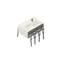
FOD2741A Fairchild Semiconductor, FOD2741A Datasheet - Page 5

FOD2741A
Manufacturer Part Number
FOD2741A
Description
Transistor Output Optocouplers Error amplifier Optocoupler
Manufacturer
Fairchild Semiconductor
Datasheet
1.FOD2741BSDV.pdf
(15 pages)
Specifications of FOD2741A
Maximum Input Diode Current
20 mA
Output Device
Transistor
Output Type
DC
Configuration
1
Input Type
DC
Maximum Collector Emitter Voltage
30 V
Maximum Collector Emitter Saturation Voltage
400 mV
Isolation Voltage
5000 Vrms
Current Transfer Ratio
200 %
Maximum Forward Diode Voltage
1.5 V
Maximum Collector Current
50 mA
Maximum Power Dissipation
145 mW
Maximum Operating Temperature
+ 85 C
Minimum Operating Temperature
- 40 C
Package / Case
PDIP W
Number Of Elements
1
Forward Voltage
1.5V
Forward Current
20mA
Collector-emitter Voltage
30V
Package Type
PDIP W
Collector Current (dc) (max)
50mA
Power Dissipation
145mW
Collector-emitter Saturation Voltage
0.4V
Pin Count
8
Mounting
Through Hole
Operating Temp Range
-40C to 85C
Operating Temperature Classification
Industrial
Lead Free Status / RoHS Status
Lead free / RoHS Compliant
Other names
FOD2741A_NL
Available stocks
Company
Part Number
Manufacturer
Quantity
Price
Company:
Part Number:
FOD2741A
Manufacturer:
FAIRCHIL
Quantity:
1 331
Part Number:
FOD2741A
Manufacturer:
FAIRCHILD/仙童
Quantity:
20 000
Part Number:
FOD2741ASD
Manufacturer:
FAIRCHILD/仙童
Quantity:
20 000
Company:
Part Number:
FOD2741ASDV
Manufacturer:
ADI
Quantity:
1 000
Part Number:
FOD2741ASDV
Manufacturer:
FAIRCHILD/仙童
Quantity:
20 000
©2004 Fairchild Semiconductor Corporation
FOD2741A, FOD2741B, FOD2741C Rev. 1.0.1
Electrical Characteristics
Isolation Characteristics
Switching Characteristics
Notes:
6. Device is considered as a two terminal device: Pins 1, 2, 3 and 4 are shorted together and Pins 5, 6, 7 and 8 are
7. Common mode transient immunity at output high is the maximum tolerable (positive) dVcm/dt on the leading edge
Symbol
Symbol
shorted together.
of the common mode impulse signal, Vcm, to assure that the output will remain high. Common mode transient
immunity at output low is the maximum tolerable (negative) dVcm/dt on the trailing edge of the common pulse
signal,Vcm, to assure that the output will remain low.
CMH
CML
V
R
BW
I
I-O
ISO
I-O
Bandwidth
Common Mode Transient
Immunity at Output HIGH
Common Mode Transient
Immunity at Output LOW
Input-Output Insulation
Leakage Current
Withstand Insulation
Voltage
Resistance (Input to Output)
Parameter
Parameter
(Continued) (T
RH = 45%, T
V
RH
V
I-O
I-O
(Fig. 7)
I
R
(I
R
LED
LED
L
L
= 3000 VDC
= 500 VDC
50%, T
= 2.2k
= 2.2k
= 0mA, Vcm = 10 V
= 1mA, Vcm = 10 V
A
Test Conditions
Test Conditions
= 25°C unless otherwise specified)
A
A
(7)
(7)
= 25°C, t = 5s,
= 25°C, t = 1 min.
5
(6)
(Fig. 8)
(Fig. 8)
(6)
PP
PP,
,
(6)
Min.
Min.
5000
Typ.
1.0
1.0
Typ.
50
10
12
Max.
Max.
1.0
www.fairchildsemi.com
kV/µs
kV/µs
Unit
Vrms
Unit
kHZ
µA


