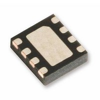
FT8010MPX Fairchild Semiconductor, FT8010MPX Datasheet - Page 4

FT8010MPX
Manufacturer Part Number
FT8010MPX
Description
Timers & Support Products Reset Timer with Configurable Delay
Manufacturer
Fairchild Semiconductor
Datasheet
1.FT8010MPX.pdf
(12 pages)
Specifications of FT8010MPX
Supply Voltage (max)
5 V
Supply Voltage (min)
2 V
Maximum Operating Temperature
+ 85 C
Minimum Operating Temperature
- 40 C
Mounting Style
SMD/SMT
Package / Case
MLP-8
Lead Free Status / RoHS Status
Lead free / RoHS Compliant
Available stocks
Company
Part Number
Manufacturer
Quantity
Price
© 2009 Fairchild Semiconductor Corporation
FT8010 • Rev. 1.0.3
Functional Description
The FT8010 reset timer uses an internal oscillator and a
two-stage, 21-bit counter to determine when the output
pins switch. Time N is set by the hard-wired logic level
of the DSR pin. N is either 7.5 ±20% seconds for
DSR=LOW or 11.25 ±20% seconds for DSR=HIGH.
Table 1.
The two input pins, /SR0 and /SR1, drive voltage
comparators that compare the voltage on the input with
the voltage set by the reference block. A low input signal
on both /SR0 and /SR1 starts the oscillator. The
oscillator sends data pulses to the digital core, which
includes the counter. There are two scenarios for
counting, as described below: short duration and long
duration. In the short-duration scenario, outputs /RST1
and RST2 are not affected. In the long duration
scenario, the outputs change state after time N. The
outputs return to their original states when a HIGH input
signal occurs on either /SR0 or /SR1.
/SR0
L
DSR
0
1
FT8010 Truth Table
/SR1
L
/RST1
Reset Timer ( +-20% )
H
H
/RST2
11.25s
7.5s
L
L
Figure 4.
The timer starts counting when both inputs go LOW. The timer stops
counting and resets when either input goes HIGH. No changes occur on
the outputs, Both /SR0 and /SR1 need to be LOW to activate (start) the
timer.
Short Duration Waveform
4
The /RST1 output is an open-drain driver. When the count
time exceeds time N, the /RST1 output drives LOW. The
RST2 output is a push-pull driver. When the count time
exceeds time N, the RST2 output drives HIGH.
The TRIG pin should be tied GND or LOW during
normal operation. The TRIG pin is a test mode pin used
for SCAN testing.
Application Note
IMPORTANT: The DSR pin must be tied to V
to provide a HIGH or LOW voltage level. The voltage
level on the DSR pin determines the length of the
configurable delay. It is important that the voltage
level on the DSR pin not change during normal
operation. The DSR must be tied to valid Vcc or
GND before SR0 or SR1 buttons go LOW.
Short Duration (t
In this case, both input /SR0 and /SR1 are LOW for a
duration t
goes LOW, the internal timer starts counting. The input
goes HIGH before time N. The timer stops counting and
resets and no changes occur on the outputs (see Figure 4).
W
which is shorter than time N. When an input
Description
W
< N)
www.fairchildsemi.com
CC
or GND


