FCH47N60NF Fairchild Semiconductor, FCH47N60NF Datasheet

MOSFET N-CH 600V 45.8A TO-247

FCH47N60NF

Manufacturer Part Number
FCH47N60NF
Description
MOSFET N-CH 600V 45.8A TO-247
Manufacturer
Fairchild Semiconductor
Series
SupreMOS™r
Datasheet

Specifications of FCH47N60NF

Input Capacitance (ciss) @ Vds
6120pF @ 100V
Fet Type
MOSFET N-Channel, Metal Oxide
Fet Feature
Logic Level Gate
Rds On (max) @ Id, Vgs
65 mOhm @ 23.5A, 10V
Drain To Source Voltage (vdss)
600V
Current - Continuous Drain (id) @ 25° C
45.8A
Vgs(th) (max) @ Id
5V @ 250µA
Gate Charge (qg) @ Vgs
157nC @ 10V
Power - Max
368W
Mounting Type
Through Hole
Package / Case
TO-247-3
Transistor Polarity
N-Channel
Resistance Drain-source Rds (on)
57.5 mOhms
Forward Transconductance Gfs (max / Min)
52 S
Drain-source Breakdown Voltage
600 V
Continuous Drain Current
45.8 A
Power Dissipation
368 W
Maximum Operating Temperature
+ 150 C
Mounting Style
Through Hole
Lead Free Status / RoHS Status
Lead free / RoHS Compliant

Available stocks

Company
Part Number
Manufacturer
Quantity
Price
Part Number:
FCH47N60NF
Manufacturer:
Fairchild Semiconductor
Quantity:
1 914
Part Number:
FCH47N60NF
Manufacturer:
TI
Quantity:
12 000
Part Number:
FCH47N60NF
Manufacturer:
ON/安森美
Quantity:
20 000
©2011 Fairchild Semiconductor Corporation
FCH47N60NF Rev. A2
*Drain current limited by maximum junction temperature
MOSFET Maximum Ratings
Thermal Characteristics
V
V
I
I
E
I
E
dv/dt
P
T
T
R
R
R
D
DM
AR
FCH47N60NF
N-Channel MOSFET, FRFET
600V, 47A, 65mΩ
Features
• R
• Ultra Low Gate Charge (Typ. Q
• Low Effective Output Capacitance
• 100% Avalanche Tested
• RoHS Compliant
J
L
DSS
GSS
AS
AR
D
θJC
θCS
θJA
, T
Symbol
Symbol
STG
DS(on)
= 57.5mΩ (Typ.) @ V
Drain to Source Voltage
Gate to Source Voltage
Drain Current
Drain Current
Single Pulsed Avalanche Energy
Avalanche Current
Repetitive Avalanche Energy
MOSFET dv/dt Ruggedness
Peak Diode Recovery dv/dt
Power Dissipation
Operating and Storage Temperature Range
Maximum Lead Temperature for Soldering Purpose,
1/8” from Case for 5 Seconds
Thermal Resistance, Junction to Case
Thermal Resistance, Case to Heat Sink (Typical)
Thermal Resistance, Junction to Ambient
G
D
S
GS
g
= 10V, I
= 121nC)
D
T
= 23.5A
C
= 25
TO-247
Parameter
Parameter
-Continuous (T
-Continuous (T
- Pulsed
(T
- Derate above 25
C
o
C unless otherwise noted
= 25
o
C)
C
C
= 25
= 100
1
o
C
o
Description
The SupreMOS MOSFET, Fairchild’s next generation of high
voltage super-junction MOSFETs, employs a deep trench filling
process that differentiates it from preceding multi-epi based
technologies. By utilizing this advanced technology and precise
process control, SupreMOS provides world class Rsp, superior
switching performance and ruggedness.
This SupreMOS MOSFET fits the industry’s AC-DC SMPS
requirements for PFC, server/telecom power, FPD TV power,
ATX power, and industrial power applications.
C)
o
C)
(Note 1)
(Note 2)
(Note 3)
G
S
D
-55 to +150
Ratings
Ratings
SupreMOS
137.4
2926
45.8
28.9
15.3
2.94
600
±30
100
368
300
0.34
0.24
3.7
50
40
www.fairchildsemi.com
January 2011
Units
W/
Units
o
V/ns
V/ns
mJ
mJ
C/W
o
o
W
V
V
A
A
A
C
C
o
C
TM
tm

Related parts for FCH47N60NF

FCH47N60NF Summary of contents

Page 1

... Thermal Resistance, Case to Heat Sink (Typical) θCS R Thermal Resistance, Junction to Ambient θJA ©2011 Fairchild Semiconductor Corporation FCH47N60NF Rev. A2 Description = 23.5A The SupreMOS MOSFET, Fairchild’s next generation of high D voltage super-junction MOSFETs, employs a deep trench filling process that differentiates it from preceding multi-epi based technologies ...

Page 2

... Notes: 1. Repetitive Rating: Pulse width limited by maximum junction temperature 15.3A 25Ω, Starting T = 25° ≤ 45.8 A, di/dt ≤ 1200A/μs, V ≤ 380V, Starting Essentially Independent of Operating Temperature Typical Characteristics FCH47N60NF Rev. A2 Package Reel Size TO-247 - unless otherwise noted C Test Conditions I = 1mA 0V ...

Page 3

... C oss iss rss 2 10 *Note 1MHz iss = shorted C oss = rss = 0 Drain-Source Voltage [V] DS FCH47N60NF Rev. A2 Figure 2. Transfer Characteristics 500 100 μ 1. 250 s Pulse Test Figure 4. Body Diode Forward Voltage 400 100 V = 10V 20V GS o *Note 120 160 Figure 6. Gate Charge Characteristics ...

Page 4

... 150 J 3. Single Pulse 0.01 0 Drain-Source Voltage [ 0.5 0.1 0.2 0.1 0.05 0.02 0.01 0.01 Single pulse 1E FCH47N60NF Rev. A2 (Continued) Figure 8. On-Resistance Variation 3.0 2.5 2.0 1.5 1.0 *Notes: 0 1mA D 0.0 100 150 200 Figure 10. Maximum Drain Current 50 μ μ 100 ...

Page 5

... FCH47N60NF Rev. A2 Gate Charge Test Circuit & Waveform Resistive Switching Test Circuit & Waveforms Unclamped Inductive Switching Test Circuit & Waveforms 5 www.fairchildsemi.com ...

Page 6

... Driver ) ( Driver ) DUT ) ( DUT ) DUT ) ( DUT ) FCH47N60NF Rev. A2 Peak Diode Recovery dv/dt Test Circuit & Waveforms + + DUT DUT Driver Driver Same Type Same Type as DUT as DUT GS GS • dv/dt controlled by R • dv/dt controlled by R • I • I controlled by pulse period controlled by pulse period ...

Page 7

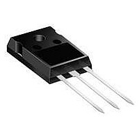
... Mechanical Dimensions FCH47N60NF Rev. A2 TO-247-3L 7 Dimensions in Millimeters www.fairchildsemi.com ...

Page 8

... PRODUCT STATUS DEFINITIONS Definition of Terms Datasheet Identification Product Status Advance Information Formative / In Design Preliminary First Production No Identification Needed Full Production Obsolete Not In Production FCH47N60NF Rev. A2 ® PowerTrench ® PowerXS™ SM Programmable Active Droop™ ® QFET QS™ Quiet Series™ RapidConfigure™ ...

Related keywords