PSMN013-100ES,127 NXP Semiconductors, PSMN013-100ES,127 Datasheet
PSMN013-100ES,127
Specifications of PSMN013-100ES,127


Related parts for PSMN013-100ES,127


PSMN013-100ES,127 Summary of contents
Page 1
... PSMN013-100ES N-channel 100 V 13.9 mΩ standard level MOSFET in I2PAK Rev. 02 — 19 February 2010 1. Product profile 1.1 General description Standard level N-channel enhancement MOSFET in I2PAK package qualified to 175C. This product is designed and qualified for use in a wide range of industrial, communications and domestic equipment. ...
Page 2
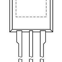
... S source mb D mounting base; connected to drain 3. Ordering information Table 3. Ordering information Type number Package Name PSMN013-100ES I2PAK PSMN013-100ES_2 Objective data sheet N-channel 100 V 13.9 mΩ standard level MOSFET in I2PAK Quick reference …continued Conditions drain-source on-state resistance T = 100 °C; see ...
Page 3
... j(init Ω unclamped 003aac512 120 P der (%) 80 40 150 200 T (°C) mb Fig 2. All information provided in this document is subject to legal disclaimers. Rev. 02 — 19 February 2010 PSMN013-100ES Min - - - -55 - ≤ 100 V; - sup 100 150 Normalized total power dissipation as a function of mounting base temperature © ...
Page 4
... Transient thermal impedance from junction to mounting base as a function of pulse duration; typical values PSMN013-100ES_2 Objective data sheet N-channel 100 V 13.9 mΩ standard level MOSFET in I2PAK Conditions see Figure 3 vertical in free air - All information provided in this document is subject to legal disclaimers. Rev. 02 — 19 February 2010 PSMN013-100ES Min Typ Max - 0.5 0 003a a d575 t p δ ...
Page 5
... DS GS see Figure 13 and see Figure see Figure 14 and see Figure 14 and MHz °C; see Figure 15 j All information provided in this document is subject to legal disclaimers. Rev. 02 — 19 February 2010 PSMN013-100ES Min Typ Max Unit 100 - - 4 100 µA - 0.06 2 µ 100 100 38.9 mΩ ...
Page 6
... V DS 003a a d577 5000 (pF) 4000 5.5 3000 5 2000 4 1000 (V) DS Fig 5. All information provided in this document is subject to legal disclaimers. Rev. 02 — 19 February 2010 PSMN013-100ES Min Typ - 109 Input and reverse transfer capacitances as a function of gate-source voltage; typical values Max Unit ...
Page 7
... V (V) GS Fig 7. 003a a d582 V GS(th) (V) 25 ° (V) GS Fig 9. All information provided in this document is subject to legal disclaimers. Rev. 02 — 19 February 2010 PSMN013-100ES 120 Forward transconductance as a function of drain current; typical values 5 4 max 3 typ 2 min 1 0 − 120 ...
Page 8
... N-channel 100 V 13.9 mΩ standard level MOSFET in I2PAK 03aa35 typ max (V) GS Fig 11. Normalized drain-source on-state resistance 003aad578 (A) D Fig 13. Gate-source voltage as a function of gate All information provided in this document is subject to legal disclaimers. Rev. 02 — 19 February 2010 PSMN013-100ES 3.2 a 2.4 1.6 0 factor as a function of junction temperature ( 50V DS 6 ...
Page 9
... N-channel 100 V 13.9 mΩ standard level MOSFET in I2PAK Q GD 003aaa508 Fig 15. Input, output and reverse transfer capacitances 100 175 ° 0.3 0.6 All information provided in this document is subject to legal disclaimers. Rev. 02 — 19 February 2010 PSMN013-100ES (pF −2 − function of drain-source voltage; typical values 003a a d584 25 °C 0.9 1.2 V ...
Page 10
... max 0.7 1.6 10.3 11 2.54 0.4 1.2 9.7 REFERENCES JEDEC JEITA TO-262 All information provided in this document is subject to legal disclaimers. Rev. 02 — 19 February 2010 PSMN013-100ES mounting base 15.0 3.30 2.6 13.5 2.79 2.2 EUROPEAN PROJECTION SOT226 ISSUE DATE 06-02-14 09-08-25 © ...
Page 11
... N-channel 100 V 13.9 mΩ standard level MOSFET in I2PAK Data sheet status Change notice Objective data sheet - Objective data sheet - All information provided in this document is subject to legal disclaimers. Rev. 02 — 19 February 2010 PSMN013-100ES Supersedes PSMN013-100ES_1 - © NXP B.V. 2010. All rights reserved ...
Page 12
... All information provided in this document is subject to legal disclaimers. Rev. 02 — 19 February 2010 PSMN013-100ES © NXP B.V. 2010. All rights reserved ...
Page 13
... Notice: All referenced brands, product names, service names and trademarks are the property of their respective owners. TrenchMOS — trademark of NXP B.V. http://www.nxp.com salesaddresses@nxp.com All information provided in this document is subject to legal disclaimers. Rev. 02 — 19 February 2010 PSMN013-100ES Trademarks © NXP B.V. 2010. All rights reserved ...
Page 14
... Please be aware that important notices concerning this document and the product(s) described herein, have been included in section ‘Legal information’. © NXP B.V. 2010. For more information, please visit: http://www.nxp.com For sales office addresses, please send an email to: salesaddresses@nxp.com All rights reserved. Date of release: 19 February 2010 Document identifier: PSMN013-100ES_2 ...