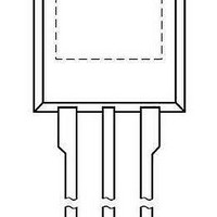
PSMN013-100ES,127 NXP Semiconductors, PSMN013-100ES,127 Datasheet - Page 8

PSMN013-100ES,127
Manufacturer Part Number
PSMN013-100ES,127
Description
MOSFET N-CH 100V I2PAK
Manufacturer
NXP Semiconductors
Datasheet
1.PSMN013-100ES127.pdf
(14 pages)
Specifications of PSMN013-100ES,127
Input Capacitance (ciss) @ Vds
3195pF @ 50V
Fet Type
MOSFET N-Channel, Metal Oxide
Fet Feature
Logic Level Gate
Rds On (max) @ Id, Vgs
13.9 mOhm @ 15A, 10V
Drain To Source Voltage (vdss)
100V
Current - Continuous Drain (id) @ 25° C
68A
Vgs(th) (max) @ Id
4V @ 1mA
Gate Charge (qg) @ Vgs
59nC @ 10V
Power - Max
170W
Mounting Type
*
Package / Case
TO-262-3 Long Leads, I²Pak, TO-262AA
Configuration
Single
Transistor Polarity
N-Channel
Resistance Drain-source Rds (on)
30 mOhms
Drain-source Breakdown Voltage
90 V
Continuous Drain Current
47 A
Power Dissipation
170 W
Mounting Style
Through Hole
Lead Free Status / RoHS Status
Lead free / RoHS Compliant
NXP Semiconductors
PSMN013-100ES_2
Objective data sheet
Fig 10. Sub-threshold drain current as a function of
Fig 12. Drain-source on-state resistance as a function
R
(mΩ)
DSon
(A)
I
10
10
10
10
10
10
D
−1
−2
−3
−4
−5
−6
30
25
20
15
10
gate-source voltage
of drain current; typical values
0
0
V
GS
(V) = 4.5
20
5
6
2
min
40
10
typ
4
60
max
V
20
All information provided in this document is subject to legal disclaimers.
GS
003aad578
I
D
(V)
03aa35
(A)
Rev. 02 — 19 February 2010
80
6
N-channel 100 V 13.9 mΩ standard level MOSFET in I2PAK
Fig 11. Normalized drain-source on-state resistance
Fig 13. Gate-source voltage as a function of gate
a
V
(V)
GS
3.2
2.4
1.6
0.8
10
0
8
6
4
2
0
factor as a function of junction temperature
charge; typical values
-60
0
15
0
PSMN013-100ES
V
DS
60
30
= 50V
120
45
© NXP B.V. 2010. All rights reserved.
Q
003aad774
003a a d583
T
G
j
(°C)
(nC)
180
60
8 of 14


