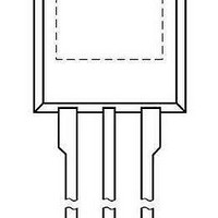
PSMN013-100ES,127 NXP Semiconductors, PSMN013-100ES,127 Datasheet - Page 4

PSMN013-100ES,127
Manufacturer Part Number
PSMN013-100ES,127
Description
MOSFET N-CH 100V I2PAK
Manufacturer
NXP Semiconductors
Datasheet
1.PSMN013-100ES127.pdf
(14 pages)
Specifications of PSMN013-100ES,127
Input Capacitance (ciss) @ Vds
3195pF @ 50V
Fet Type
MOSFET N-Channel, Metal Oxide
Fet Feature
Logic Level Gate
Rds On (max) @ Id, Vgs
13.9 mOhm @ 15A, 10V
Drain To Source Voltage (vdss)
100V
Current - Continuous Drain (id) @ 25° C
68A
Vgs(th) (max) @ Id
4V @ 1mA
Gate Charge (qg) @ Vgs
59nC @ 10V
Power - Max
170W
Mounting Type
*
Package / Case
TO-262-3 Long Leads, I²Pak, TO-262AA
Configuration
Single
Transistor Polarity
N-Channel
Resistance Drain-source Rds (on)
30 mOhms
Drain-source Breakdown Voltage
90 V
Continuous Drain Current
47 A
Power Dissipation
170 W
Mounting Style
Through Hole
Lead Free Status / RoHS Status
Lead free / RoHS Compliant
NXP Semiconductors
5. Thermal characteristics
Table 5.
PSMN013-100ES_2
Objective data sheet
Symbol
R
R
Fig 3.
th(j-mb)
th(j-a)
Z
(K/W)
th (j-mb)
10
10
10
10
-1
-2
-3
-4
1
1e -6
values
Transient thermal impedance from junction to mounting base as a function of pulse duration; typical
δ = 0.5
0.2
0.1
0.05
0.02
s ingle s hot
Thermal characteristics
Parameter
thermal resistance from
junction to mounting
base
thermal resistance from
junction to ambient
10
-5
Conditions
see
vertical in free air
10
-4
Figure 3
All information provided in this document is subject to legal disclaimers.
Rev. 02 — 19 February 2010
10
N-channel 100 V 13.9 mΩ standard level MOSFET in I2PAK
-3
10
-2
10
-1
PSMN013-100ES
Min
-
-
P
1
Typ
0.5
60
t
p
T
© NXP B.V. 2010. All rights reserved.
t
p
(s )
003a a d575
δ =
Max
0.9
-
T
t
p
t
10
Unit
K/W
K/W
4 of 14


