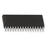
IS62C1024AL-35QLI INTEGRATED SILICON SOLUTION (ISSI), IS62C1024AL-35QLI Datasheet - Page 3

IS62C1024AL-35QLI
Manufacturer Part Number
IS62C1024AL-35QLI
Description
IC, SRAM, 1MBIT, 35NS, SOP-32
Manufacturer
INTEGRATED SILICON SOLUTION (ISSI)
Datasheet
1.IS62C1024AL-35TLI.pdf
(11 pages)
Specifications of IS62C1024AL-35QLI
Memory Size
1Mbit
Memory Configuration
128K X 8
Access Time
35ns
Supply Voltage Range
4.5V To 5.5V
Memory Case Style
SOP
No. Of Pins
32
Operating Temperature Range
-40°C To +85°C
Lead Free Status / RoHS Status
Lead free / RoHS Compliant
Available stocks
Company
Part Number
Manufacturer
Quantity
Price
Company:
Part Number:
IS62C1024AL-35QLI
Manufacturer:
ISSI
Quantity:
1 000
Company:
Part Number:
IS62C1024AL-35QLI
Manufacturer:
ISSI
Quantity:
2 148
Part Number:
IS62C1024AL-35QLI
Manufacturer:
ISSI
Quantity:
20 000
Company:
Part Number:
IS62C1024AL-35QLI-TR
Manufacturer:
ISSI
Quantity:
1 000
IS62C1024AL
IS65C1024AL
ABSOLUTE MAXIMUM RATINGS
t
P
I
Notes:
1. Stress greater than those listed under ABSOLUTE MAXIMUM RATINGS may cause permanent damage to the device. This is a
DC ELECTRICAL CHARACTERISTICS
V
V
V
I
I
Note:
1. V
V
Integrated Silicon Solution, Inc. — www.issi.com —
Rev. H
06/26/08
CAPACITANCE
c
Notes:
1. Tested initially and after any design or process changes that may affect these parameters.
2. Test conditions: T
Symbol
V
stress rating only and functional operation of the device at these or any other conditions above those indicated in the operational
sections of this specification is not implied. Exposure to absolute maximum rating conditions for extended periods may affect reli-
ability.
Symbol Parameter
V
Symbol
c
Il
out
lI
lo
Ih
stg
(min.) = -0.3V DC; V
term
t
oh
ol
Ih
Il
In
out
(max.) = V
Output HIGH Voltage
Output LOW Voltage
Input HIGH Voltage
Input LOW Voltage
Input Leakage
Output Leakage
DD
Parameter
Terminal Voltage with Respect to GND
Storage Temperature
Power Dissipation
DC Output Current (LOW)
+ 0.3V DC; V
a
Parameter
Input Capacitance
Output Capacitance
(1,2)
= 25°c, f = 1 MHz, V
Il
(min.) = -2.0V AC (pulse width -2.0 ns). Not 100% tested.
Ih
(max.) = V
(1)
DD
DD
+ 2.0V AC (pulse width -2.0 ns). Not 100% tested.
Test Conditions
V
V
GND ≤ V
GND ≤ V
CE1 = V
CE2 = V
WE = V
= 5.0V.
DD
DD
(1)
= Min., I
= Min., I
Il
Ih
Il
In
out
, or OE = V
, or
(Over Operating Range)
≤ V
oh
ol
≤ V
Conditions
V
DD
V
= 2.1 mA
= –1.0 mA
out
DD
1-800-379-4774
In
= 0V
= 0V
Ih
or
Options
–0.5 to +7.0
–65 to +125
Com.
Com.
Auto.
Auto.
Ind.
Ind.
Value
1.0
20
Max.
Min.
-0.5
2.4
2.2
6
8
—
-1
-2
-5
-1
-2
-5
V
DD
Max.
0.4
0.8
—
1
2
5
1
2
5
+ 0.5
Unit
Unit
mA
°C
W
pF
pF
V
Unit
µA
µA
V
V
V
V
3


