TLE4925 Infineon Technologies, TLE4925 Datasheet
TLE4925
Specifications of TLE4925
SP000269338
TLE4925
TLE4925INTB
TLE4925X
Available stocks


Related parts for TLE4925

TLE4925 Summary of contents
Page 1
... TLE4925 TLE4925C General Information The TLE4925/TLE4925C is an active Hall sensor suited to detect the motion and position of ferromagnetic and permanent magnet structures. An additional self- calibration module has been implemented to achieve optimum accuracy during normal running operation. It comes in a three-pin package for the supply voltage and an open drain output ...
Page 2
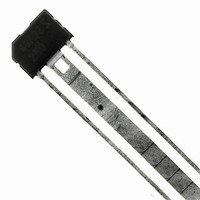
Figure 1: Pin configuration in PG-SSO-3-6 and PG-SSO-3-9 Pin definition and Function Pin No. Symbol GND 3 Q Functional Description The differential Hall sensor IC detects the motion and position of ferromagnetic and permanent magnet structures ...
Page 3
... Figure 2: Block Diagram of TLE4925/TLE4925C Circuit Description The TLE4925/TLE4925C is comprised of a supply voltage regulator, a pair of hall probes, spaced at 2.5mm, differential amplifier, noise-shaping filter, comparator, advanced digital signal processor (DSP), A/D and D/A converter and an open drain output. Startup mode: The differential signal is digitized in the A/D converter and fed into the dsp part of the circuit ...
Page 4
Running mode: In running mode the output is triggered by the comparator. An offset cancellation feedback loop is formed by the A/D converter, dsp and offset cancellation D/A converter. In running mode switching always occurs at zero-crossing only ...
Page 5
Absolute Maximum Ratings No. Parameter Symbol 1.1.1 Supply voltage V 1.1.2 Supply current 1.1.3 Output OFF voltage V 1.1.4 Output ON voltage V 1.1.5 Continuous output current 1.1.6 Junction temperature 1.1.7 Storage temperature T 1.1.8 Thermal resistance R junction-air ...
Page 6
ESD Protection No. Parameter 1.2.1 ESD – protection PG-SSO-3-9 PG-SSO-3-6 2.1 Operating Range No. Parameter 2.1.1 Supply voltage 2.1.2 Supply voltage ripple 2.1.3 Continuous output OFF voltage 2.1.4 Continuous output ON current 2.1.5 Power on time 2 Output of ...
Page 7
... Junction temperature limit for output protection 2.2.8 Output rise time TLE4925C (PG-SSO-3-9) TLE4925 (PG-SSO-3-6) 3 value of capacitor: 4.7nF±10%; (excluded drift due to temperature); ceramic: X7R; maximum voltage: 100V. The rise time is defined as the time between the 10 and 90% value. Data Sheet T -40 ...
Page 8
... Output fall time TLE4925C (PG-SSO-3-9) TLE4925 (PG-SSO-3-6) 2.2.10 delay time Falling edge Rising edge 2.2.11 Temperature drift of delay time of output to magnetic edge 2.2.12 Frequency range 2.2.13 Oscillator frequency 2.2.14 Offset recalibration time after last output change 2.2.15 Clamping voltage V -Pin S 2 ...
Page 9
Magnetic Characteristics No. Parameter 2.3.1 Bias preinduction 2.3.2 Differential bias induction 2.3.3 Minimum signal amplitude 2.3.4 Maximum signal amplitude 2.3.5 Resistivity against mechanical stress (piezo) Note: The listed characteristics are ensured over the operating range of the integrated circuit. ...
Page 10
Signal Jitter in running mode at power supply of Vs=13V and ripple ±3V; 1 sigma value* 3.1.6 Effective noise value of the magnetic switching points, 1 sigma value 3.1.7 Uncalibrated phase error Magnetic edge 1-2 rd After 3 edge ...
Page 11
B B max ∆B 50% ∆ min ∆ ∆ Q-High 90% 50 10% V Q-Low Figure 4 Switching direction Signal ∆ ∑ σ σ = ⋅ ...
Page 12
... Two possible applications are shown in Figure 6 and Figure 7 (Toothed and Magnet Wheel). The difference between two-wire and three-wire application is shown in Figure 10 for the TLE4925C and in Figure 11 for the TLE4925. Gear Tooth Sensing In the case of ferromagnetic toothed wheel application the IC has to be biased by the south or north pole of a permanent magnet (e.g. SmCO VX145)) with the dimensions 8 mm × ...
Page 13
... Hall Sensor 1 Hall Sensor 1 Signal Processing Circuitry Figure 8 TLE4925/TLE4925C, with Ferromagnetic Toothed Wheel S Hall Sensor 1 Signal Processing Circuitry Figure 9 TLE4925/TLE4925C, with Magnet Wheel Data Sheet Gear Wheel S (N) N (S) N (S) S (N) AEA01261 Magnet Wheel S N AEA01262 Page Hall Sensor 2 Permanent Magnet ...
Page 14
... R L ≥200Ω for example =1,2kΩ L Figure 10 Application Circuits TLE4925C (capacitors added in package) Data Sheet =1,2kΩ R =120Ω Page 10/02/2005 ...
Page 15
... R L Three-wire-application 470 nF for example : R = 330 ≥200Ω for example ... 330 R =1,2kΩ Figure 11 Application Circuits TLE4925 (capacitors to be added externally) Data Sheet =1,2kΩ R =120Ω GND 4 Sensor Page Line SIGNAL Mainframe AES01264 10/02/2005 ...
Page 16
S (N) N (S) Pin 3 ( Crankshaft Wheel Profile Enabling point for releasing output: B1-B2<∆B output OFF (V =HIGH). Q Enabling point for operate point: B1-B2>∆B output ON (V =LOW). Q ∆B =|∆B -∆B | HYS ENOP ...
Page 17
Appendix: Calculation of mechanical errors: ϕ ∆ϕ ∆ϕ Systematic Phase Error The systematic error comes in because of the delay-time between the threshold point and the time when the output is switching. It can be calculated as follows: ϕ ... ...
Page 18
Systematic Phase Error ∆ϕ The systematic phase error includes the error due to the variation of the delay time with temperature and the error caused by the resolution of the threshold. It can be calculated in the following way: ∆ϕ ...
Page 19
Tj=25°C in ° (1Sigma) Jitter_typ ϕ ... maximum phase jitter at Tj=175°C in ° (3Sigma) Jitter_max ϕ ∂ ... inverse of the magnetic slope of the edge in °/T ∂ ... typical ...
Page 20
Electro Magnetic Compatibility - (values depend on R Ref. ISO 7637-1; see test circuit of figure 4 and 5; ∆B = 10mT (ideal sinusoidal signal No. Parameter 4.1.1 Testpulse 1 Testpulse 2 Testpulse 3a Testpulse 3b Testpulse ...
Page 21
... R Series 200Ω C Int-package 4 EMC Figure 13: Test Circuit for EMC tests (TLE4925C) – PG-SSO-3-9 Package R Series 200Ω C Ext1 V EMC Figure 14: Test Circuit for EMC tests (TLE4925) – PG-SSO-3-6 Package Data Sheet GND C Int-package R Load 4.7nF GND Load Page 1.2 kΩ ...
Page 22
PG-SSO-3-9 (Plastic Green Single Small Outline) Figure 15 Package Dimensions (PG-SSO-3-9) Data Sheet Page 10/02/2005 ...
Page 23
Figure 16 Hall probe spacing in the PG-SSO-3-9 package Data Sheet Page 10/02/2005 ...
Page 24
Figure 17 Tape Loading Orientation in the PG-SSO-3-9 package Data Sheet Page 10/02/2005 ...
Page 25
Figure 18 Package Dimensions (PG-SSO-3-6) Data Sheet Page 10/02/2005 ...
Page 26
Figure 19 Hall probe spacing in the PG-SSO-3-6 package Figure 20 Tape Loading Orientation in the PG-SSO-3-6 package Data Sheet Page 10/02/2005 ...
Page 27
Appendix A: Marking & data matrix code information: Product is RoHS (restriction of hazardous substances) compliant when marked with letter “G” in front or after the date code marking. As mentioned in information note N° 136/03 a data matrix code ...
Page 28
... Update package drawing: parallelism 27 Update comparison mask writing/laser writing Infineon Technologies AG © Infineon Technologies AI SC All Rights Reserved. http://www.infineon.com/products/sensors We Listen to Your Comments Any information within this document that you feel is wrong, unclear or missing at all? Your feedback will help us to continuously improve the quality of this document. ...