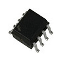
HCPL062N Fairchild Semiconductor, HCPL062N Datasheet - Page 5

HCPL062N
Manufacturer Part Number
HCPL062N
Description
OPTOCOUPLER, LOGIC GATE, 2500VRMS
Manufacturer
Fairchild Semiconductor
Datasheet
1.HCPL062N.pdf
(13 pages)
Specifications of HCPL062N
No. Of Channels
2
Optocoupler Output Type
Logic Gate
Input Current
15mA
Output Voltage
7V
Opto Case Style
SOIC
No. Of Pins
8
Rise Time
16ns
Output Voltage Max
7V
Isolation Voltage
2.5kV
Number Of Elements
2
Input Type
DC
Output Type
Open Collector
Baud Rate
10Mbps
Forward Voltage
1.75V
Forward Current
50mA
Output Current
15mA
Package Type
SOIC N
Operating Temp Range
-40C to 85C
Power Dissipation
85mW
Propagation Delay Time
90ns
Pin Count
8
Mounting
Surface Mount
Reverse Breakdown Voltage
5V
Operating Temperature Classification
Industrial
Rohs Compliant
Yes
Lead Free Status / RoHS Status
Lead free / RoHS Compliant
Lead Free Status / RoHS Status
Lead free / RoHS Compliant
Available stocks
Company
Part Number
Manufacturer
Quantity
Price
Company:
Part Number:
HCPL062N
Manufacturer:
FSC
Quantity:
1 878
Part Number:
HCPL062N
Manufacturer:
FAIRCHILD/仙童
Quantity:
20 000
Company:
Part Number:
HCPL062NR2
Manufacturer:
FSC
Quantity:
7 500
HCPL062N Rev. 1.0.0
Transfer Characteristics
Isolation Characteristics
Notes:
3. All typical values are at V
4. t
5. t
6. t
7. t
8. CM
9. CM
10. Device considered a two-terminal device: Pins 1,2,3 and 4 shorted together, and Pins 5,6,7 and 8 shorted together.
11. The power supply bypass capacitors must be no further than 3mm from the leads of the optocoupler. A low
Symbol
Symbol
V
pulse to the 1.5V level on the LOW to HIGH transition of the output voltage pulse.
pulse to the 1.5V level on the HIGH to LOW transition of the output voltage pulse.
state (i.e., V
output state (i.e., V
inductance ground plane width of with ≤ 5nHy of series lead inductance is required.
I
V
PLH
PHL
r
f
R
C
FT
I
OL
– Fall time is measured from the 10% to the 90% levels on the HIGH to LOW transition of the output pulse.
I-O
– Rise time is measured from the 90% to the 10% levels on the LOW to HIGH transition of the output pulse.
ISO
I-O
I-O
H
L
– Propagation delay is measured from the 3.75 mA level on the HIGH to LOW transition of the input current
– Propagation delay is measured from the 3.75 mA level on the LOW to HIGH transition of the input current
– The maximum tolerable rate of fall of the common mode voltage to ensure the output will remain in the low
– The maximum tolerable rate of rise of the common mode voltage to ensure the output will remain in the high
Low Level Output Voltage
Input Threshold Current
Input-Output
Insulation Leakage Current
Withstand Insulation Test
Voltage
Resistance (Input to Output)
Capacitance (Input to Output)
DC Characteristics
OUT
> 2.0 V). Measured in volts per microsecond (V/µs).
Characteristics
OUT
< 0.8 V). Measured in volts per microsecond (V/µs).
CC
(T
(T
A
A
= 3.3V, T
= -40°C to +85°C Unless otherwise specified.)
= -40°C to +85°C Unless otherwise specified.)
A
V
V
CC
CC
= 25°C unless otherwise specified.
= 3.3V, I
= 3.3V, V
Relative humidity = 45%
T
V
R
I
Note 10
V
f = 1MHz, Note 10
I-O
A
I-O
I-O
H
Test Conditions
= 25°C, t = 5 sec.
< 50%, T
≤ 2µA, t = 1 min.,
Test Conditions
= 3000 VDC, Note 10
= 500V, Note 10
F
O
= 5mA, I
= 0.6V, I
5
A
= 25°C
OL
OL
= 13mA
= 13mA
Min.
2500
–
–
–
Min.
–
–
Typ.
10
Typ.
0.6
–
–
12
(3)
–
–
(3)
Max.
1.0
Max.
–
–
–
0.6
5
www.fairchildsemi.com
V
Unit
Unit
µA
RMS
pF
mA
Ω
V


