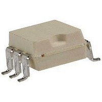
MOC3051-M Fairchild Semiconductor, MOC3051-M Datasheet - Page 6

MOC3051-M
Manufacturer Part Number
MOC3051-M
Description
OPTOCOUPLER, TRIAC, 7500V
Manufacturer
Fairchild Semiconductor
Datasheet
1.MOC3051-M.pdf
(13 pages)
Specifications of MOC3051-M
No. Of Channels
1
Optocoupler Output Type
Phototriac
Input Current
10mA
Output Voltage
600V
Opto Case Style
DIP
No. Of Pins
6
Peak Reflow Compatible (260 C)
Yes
Isolation Voltage
7.5kV
Lead Free Status / RoHS Status
Lead free / RoHS Compliant
©2005 Fairchild Semiconductor Corporation
MOC3051M, MOC3052M Rev. 1.0.5
Minimum LED Off Time in Phase Control
Applications
In Phase control applications one intends to be able to
control each AC sine half wave from 0° to 180°. Turn on
at 0° means full power and turn on at 180° means zero
power. This is not quite possible in reality because triac
driver and triac have a fixed turn on time when activated
at zero degrees. At a phase control angle close to 180°
the driver’s turn on pulse at the trailing edge of the AC
sine wave must be limited to end 200ms before AC zero
cross as shown in Figure 5. This assures that the triac
driver has time to switch off. Shorter times may cause
loss of control at the following half cycle.
I
Triac drivers with good noise immunity (dv/dt static) have
internal noise rejection circuits which prevent false
FT
versus dv/dt
0.9
0.8
0.7
0.6
0.5
0.4
0.3
0.2
0.1
1.0
0
Figure 5. Minimum Time for LED Turn–Off to Zero
- 40
Figure. 6 Holding Current, I
0
-30 -20 -10 0
T A - AMBIENT TEMPERATURE (
Cross of AC Trailing Edge
10 20 30 40 50 60 70 80
LED PW
180
LED turn off min. 200 s
H
vs. Temperature
AC Sine
LED Current
o
C)
6
triggering of the device in the event of fast raising line
voltage transients. Inductive loads generate a commutat-
ing dv/dt that may activate the triac drivers noise sup-
pression circuits. This prevents the device from turning
on at its specified trigger current. It will in this case go
into the mode of “half waving” of the load. Half waving of
the load may destroy the power triac and the load.
Figure 8 shows the dependency of the triac drivers I
versus the reapplied voltage rise with a Vp of 400V. This
dv/dt condition simulates a worst case commutating
dv/dt amplitude.
It can be seen that the I
commutating dv/dt reaches 1000V/ms. The data sheet
specified I
inductive loads and load factors.
1000
100
0.1
10
1
-40
1.5
1.4
1.3
1.2
1.1
0.9
0.8
0.7
0.6
0.5
0.001
1
Figure. 7 Leakage Current, I
FT
Figure. 8 LED Trigger Current, I
-20
is therefore applicable for all practical
0.01
T A - AMBIENT TEMPERATURE (
0
0.1
dv/dt (V/ms)
FT
20
1
does not change until a
40
DRM
10
NORMALIZED TO:
vs. Temperature
100
I FT at 3 V
FT
60
o
www.fairchildsemi.com
vs. dv/dt
C)
1000
80
10000
FT
100


