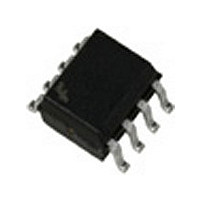
FOD0708 Fairchild Semiconductor, FOD0708 Datasheet - Page 3

FOD0708
Manufacturer Part Number
FOD0708
Description
OPTOCOUPLER, LOGIC GATE, 2500VRMS
Manufacturer
Fairchild Semiconductor
Datasheet
1.FOD0708.pdf
(12 pages)
Specifications of FOD0708
No. Of Channels
1
Optocoupler Output Type
Gate Drive
Input Current
16mA
Output Voltage
5V
Opto Case Style
SOIC
No. Of Pins
8
Length/height, External
3.63mm
Isolation Voltage
2.5kV
Number Of Elements
1
Input Type
DC
Output Type
Push-Pull
Baud Rate
15Mbps
Forward Voltage
1.8V
Forward Current
20mA
Output Current
2mA
Package Type
SOIC N
Operating Temp Range
-40C to 100C
Power Dissipation
85mW
Propagation Delay Time
60ns
Pin Count
8
Mounting
Surface Mount
Operating Temperature Classification
Industrial
Lead Free Status / RoHS Status
Lead free / RoHS Compliant
Lead Free Status / RoHS Status
Lead free / RoHS Compliant
©2003 Fairchild Semiconductor Corporation
FOD0708, FOD0738 Rev. 1.0.8
Switching Characteristics
4.5 V ≤ V
*All typicals at T
Isolation Characteristics
*All typical values are at V
Notes:
1. Propagation delay time, high to low (t
2. Pulse width distoration is defined as the absolute difference between the high to low and low to high propagation
3. Propagation delay skew, t
4. CM
5. CM
6. Isolation voltage, V
Characteristics
Input-Output Insulation
Leakage Current
Withstand Insulation
Test Voltage
Resistance (Input to Output)
Capacitance (Input to Output)
Symbol
| PWD |
| CM
| CM
the 2.5V level of the falling edge of the output voltage signal. Propagation delay time, low to high (t
from the 50% level on the falling edge of the input pulse to the 2.5V level of the rising edge of the output voltage
signal.
delay times, | t
recommended operating range of the device.
state, (i,e., V
state, (i,e., V
pins 5,6,7,8 are common.
t
t
t
PW
PSK
PHL
PLH
t
t
R
F
H
H
L
L
– The maximum tolerated rate of fall of the common mode voltage to ensure the output will remain in the low
– The maximum tolerated rate of rise of the common mode voltage to ensure the output will remain in the high
DD
|
|
≤ 5.5 V. All typical specifications are at T
Propagation Delay Time to
Logic Low Output
Propagation Delay Time to
Logic High Output
Pulse Width
Pulse Width Distortion
Propagation Delay Skew
Output Rise Time (10%–90%) I
Output Fall Time (90%–10%)
Common Mode Transient
Immunity at Logic High
Output
Common Mode Transient
Immunity at Logic Low Output
A
OUT
OUT
= 25°C and V
PHL
> 2.0V) Measured in kilovolts per microsecond (kV/µs).
< 0.8V). Measured in kilovolts per microsecond (kV/µs).
Parameter
– t
ISO
PLH
, is an internal device dielectric breakdown rating. For this test, pins 1,2,3,4 are common, and
CC
|.
= 5 V, T
PSK
DD
, is defined as the worst case difference in t
= 5V unless otherwise noted.
Relative humidity = 45%,
T
V
T
V
f = 1MHz (Note 6)
I
A
A
(T
I-O
I-O
I-O
A
= 25°C, t = 5s,
= 25°C, t = 1 min. (Note 6)
A
= 25°C
Over recommended temperature (T
≤ 10µA, R
= 3000 VDC (Note 6)
= 500V (Note 6)
= -40°C to +100°C Unless otherwise specified.)
PHL
), is measured from the 50% level on the rising edge of the input pulse to
I
CMOS Signal Levels (Note 1) (Fig. 10)
I
CMOS Signal Levels,
(Note 1) (Fig. 10)
I
CMOS Signal Levels (Note 2)
I
CMOS Signal Levels (Note 3)
CMOS Signal Levels
I
CMOS Signal Levels
V
(Note 4) (Fig. 11)
V
(Note 5) (Fig. 11)
F
F
F
F
F
F
CM
CM
Test Conditions Symbol
= 12mA, C
= 12mA, C
= 12mA, C
= 12mA, C
= 12mA, C
= 12mA, C
H
= 1000V, T
= 1000V, T
< 50%,
A
= 25°C, V
Test Conditions
L
L
L
L
L
L
3
= 15pF
= 15pF
= 15pF,
= 15pF,
= 15pF,
= 15pF,
A
A
= 25°C, I
= 25°C, I
DD
= +5 V.
FOD0708
FOD0738
V
R
C
I
F
I-O
F
ISO
I-O
I-O
= 12mA,
= 0mA,
A
= –40°C to +100°C) and
PHL
2500
Min
or t
PLH
Min. Typ.* Max.
100
20
13
11
25
25
0
between units within the
Typ.*
10
0.6
12
12
50
50
8
PLH
Max
1.0
60
60
60
30
40
), is measured
www.fairchildsemi.com
Units
V
kV/µs
kV/µs
Unit
µA
pF
RMS
ns
ns
ns
ns
ns
ns
ns
Ω


