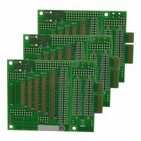
AC164139 Microchip Technology, AC164139 Datasheet - Page 216

AC164139
Manufacturer Part Number
AC164139
Description
Graphics Display Prototype Board Graphics
Manufacturer
Microchip Technology
Specifications of AC164139
Main Purpose
LCD Development
Embedded
No
Utilized Ic / Part
PICtail™ Plus Board
Lead Free Status / RoHS Status
Lead free / RoHS Compliant
Secondary Attributes
-
Primary Attributes
-
Lead Free Status / RoHS Status
Lead free / RoHS Compliant
Available stocks
Company
Part Number
Manufacturer
Quantity
Price
Company:
Part Number:
AC164139
Manufacturer:
Microchip Technology
Quantity:
135
- Current page: 216 of 408
- Download datasheet (4Mb)
PIC24FJ256DA210 FAMILY
REGISTER 15-2:
DS39969B-page 216
bit 15
bit 7
Legend:
R = Readable bit
-n = Value at POR
bit 15-13
bit 12
bit 11
bit 10
bit 9
bit 8
bit 7
bit 6
bit 5
Note 1:
SSEN
R/W-0
U-0
—
2:
3:
4:
(4)
If DISSCK = 0, SCKx must be configured to an available RPn pin. See Section 10.4 “Peripheral Pin
Select (PPS)” for more information.
If DISSDO = 0, SDOx must be configured to an available RPn pin. See Section 10.4 “Peripheral Pin
Select (PPS)” for more information.
The CKE bit is not used in the Framed SPI modes. The user should program this bit to ‘0’ for the Framed
SPI modes (FRMEN = 1).
If SSEN = 1, SSx must be configured to an available RPn/PRIn pin. See Section 10.4 “Peripheral Pin
Select (PPS)” for more information.
Unimplemented: Read as ‘0’
DISSCK: Disable SCKx Pin bit (SPI Master modes only)
1 = Internal SPI clock is disabled; pin functions as I/O
0 = Internal SPI clock is enabled
DISSDO: Disable SDOx Pin bit
1 = SDOx pin is not used by the module; pin functions as I/O
0 = SDOx pin is controlled by the module
MODE16: Word/Byte Communication Select bit
1 = Communication is word-wide (16 bits)
0 = Communication is byte-wide (8 bits)
SMP: SPIx Data Input Sample Phase bit
Master mode:
1 = Input data sampled at the end of data output time
0 = Input data sampled at the middle of data output time
Slave mode:
SMP must be cleared when SPIx is used in Slave mode.
CKE: SPIx Clock Edge Select bit
1 = Serial output data changes on transition from active clock state to Idle clock state (see bit 6)
0 = Serial output data changes on transition from Idle clock state to active clock state (see bit 6)
SSEN: Slave Select Enable (Slave mode) bit
1 = SSx pin is used for Slave mode
0 = SSx pin is not used by the module; pin is controlled by the port function
CKP: Clock Polarity Select bit
1 = Idle state for the clock is a high level; active state is a low level
0 = Idle state for the clock is a low level; active state is a high level
MSTEN: Master Mode Enable bit
1 = Master mode
0 = Slave mode
R/W-0
CKP
U-0
—
SPI
X
CON1: SPIx CONTROL REGISTER 1
W = Writable bit
‘1’ = Bit is set
MSTEN
R/W-0
U-0
—
DISSCK
(2)
SPRE2
R/W-0
R/W-0
(3)
(1)
U = Unimplemented bit, read as ‘0’
‘0’ = Bit is cleared
(4)
DISSDO
SPRE1
R/W-0
R/W-0
(2)
(1)
MODE16
SPRE0
R/W-0
R/W-0
2010 Microchip Technology Inc.
x = Bit is unknown
PPRE1
R/W-0
R/W-0
SMP
PPRE0
CKE
R/W-0
R/W-0
(3)
bit 8
bit 0
Related parts for AC164139
Image
Part Number
Description
Manufacturer
Datasheet
Request
R

Part Number:
Description:
Manufacturer:
Microchip Technology Inc.
Datasheet:

Part Number:
Description:
Manufacturer:
Microchip Technology Inc.
Datasheet:

Part Number:
Description:
Manufacturer:
Microchip Technology Inc.
Datasheet:

Part Number:
Description:
Manufacturer:
Microchip Technology Inc.
Datasheet:

Part Number:
Description:
Manufacturer:
Microchip Technology Inc.
Datasheet:

Part Number:
Description:
Manufacturer:
Microchip Technology Inc.
Datasheet:

Part Number:
Description:
Manufacturer:
Microchip Technology Inc.
Datasheet:

Part Number:
Description:
Manufacturer:
Microchip Technology Inc.
Datasheet:


