AC164139 Microchip Technology, AC164139 Datasheet - Page 24
AC164139
Manufacturer Part Number
AC164139
Description
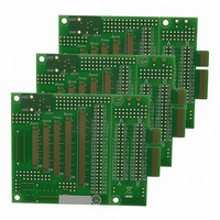
Graphics Display Prototype Board Graphics
Manufacturer
Microchip Technology
Specifications of AC164139
Main Purpose
LCD Development
Embedded
No
Utilized Ic / Part
PICtail™ Plus Board
Lead Free Status / RoHS Status
Lead free / RoHS Compliant
Secondary Attributes
-
Primary Attributes
-
Lead Free Status / RoHS Status
Lead free / RoHS Compliant
Available stocks
Company
Part Number
Manufacturer
Quantity
Price
Company:

Part Number:
AC164139
Manufacturer:
Microchip Technology
Quantity:
135


PIC24FJ256DA210 FAMILY
TABLE 1-3:
DS39969B-page 24
CN81
CN82
CN83
CN84
CTEDG1
CTEDG2
CTPLS
CV
D+
D-
DMH
DMLN
DPH
DPLN
ENVREG
GCLK
GD0
GD1
GD2
GD3
GD4
GD5
GD6
GD7
GD8
GD9
GD10
GD11
GD12
GD13
GD14
GD15
GEN
GPWR
HSYNC
INT0
MCLR
OSCI
OSCO
Legend:
Note 1:
Function
REF
2:
3:
4:
TTL = TTL input buffer
ANA = Analog level input/output
The alternate EPMP pins are selected when the ALTPMP (CW3<12>) bit is programmed to ‘0’.
The PMSC2 signal will replace the PMA15 signal on the 15-pin PMA when CSF<1:0> = 01 or 10.
The PMCS1 signal will replace the PMA14 signal on the 14-pin PMA when CSF<1:0> = 10.
The alternate V
TQFP/QFN
64-Pin
37
36
23
37
36
52
60
62
63
31
32
44
45
49
58
59
51
46
39
40
—
—
28
27
29
46
42
50
43
57
61
43
53
64
2
3
6
8
7
PIC24FJ256DA210 FAMILY PINOUT DESCRIPTIONS (CONTINUED)
Pin Number
REF
100-Pin
TQFP
pins selected when the ALTVREF (CW1<5>) bit is programmed to ‘0’.
95
57
56
42
41
43
34
57
56
72
68
77
69
86
39
52
21
22
23
76
53
69
77
32
33
47
48
91
27
97
72
13
63
64
1
1
6
8
7
121-Pin
BGA
H10
H10
A10
E10
K11
A11
E10
A10
J11
J11
J10
F11
C4
B2
K7
D9
E9
B2
D1
E2
H2
E4
K4
K9
C5
A3
D9
L7
L5
L6
L4
L9
F1
F9
J7
J7
J1
J2
J3
I/O
I/O
I/O
O
O
O
O
O
O
O
O
O
O
O
O
O
O
O
O
O
O
O
O
O
O
O
O
O
O
O
I
I
I
I
I
I
I
I
I
I
Buffer
Input
ANA
ANA
ANA
ANA
ST
ST
ST
ST
ST
ST
ST
—
—
—
—
—
—
—
—
—
—
—
—
—
—
—
—
—
—
—
—
—
—
—
—
—
—
—
—
ST = Schmitt Trigger input buffer
I
2
C™ = I
Interrupt-on-Change Inputs.
CTMU External Edge Input 1.
CTMU External Edge Input 2.
CTMU Pulse Output.
Comparator Voltage Reference Output.
USB Differential Plus Line (internal transceiver).
USB Differential Minus Line (internal transceiver).
D- External Pull-up Control Output.
D- External Pull-down Control Output.
D+ External Pull-up Control Output.
D+ External Pull-down Control Output.
Voltage Regulator Enable.
Graphics Display Pixel Clock.
Graphics Controller Data Output.
Graphics Display Enable Output.
Graphics Display Power System Enable.
Graphics Display Horizontal Sync Pulse.
External Interrupt Input.
Master Clear (device Reset) Input. This line is brought low
to cause a Reset.
Main Oscillator Input Connection.
Main Oscillator Output Connection.
2
C/SMBus input buffer
Description
2010 Microchip Technology Inc.
Related parts for AC164139
Image
Part Number
Description
Manufacturer
Datasheet
Request
R

Part Number:
Description:
Manufacturer:
Microchip Technology Inc.
Datasheet:
Part Number:
Description:
Manufacturer:
Microchip Technology Inc.
Datasheet:
Part Number:
Description:
Manufacturer:
Microchip Technology Inc.
Datasheet:
Part Number:
Description:
Manufacturer:
Microchip Technology Inc.
Datasheet:
Part Number:
Description:
Manufacturer:
Microchip Technology Inc.
Datasheet:
Part Number:
Description:
Manufacturer:
Microchip Technology Inc.
Datasheet:
Part Number:
Description:
Manufacturer:
Microchip Technology Inc.
Datasheet:
Part Number:
Description:
Manufacturer:
Microchip Technology Inc.
Datasheet: