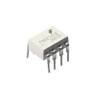
HCPL2611 Fairchild Semiconductor, HCPL2611 Datasheet

HCPL2611
Specifications of HCPL2611
Available stocks
Related parts for HCPL2611
HCPL2611 Summary of contents
Page 1
... A maximum input signal of 5mA will provide a minimum output sink current of 13mA (fan out of 8). An internal noise shield provides superior common mode rejection of typically 10kV/µs. The HCPL2601 and HCPL2631 has a minimum CMR of 5kV/µs. The HCPL2611 has a minimum CMR of 10kV/µs. Package Outlines ...
Page 2
... N Fan Out (TTL load) *6.3mA is a guard banded value which allows for at least 20% CTR degradation. Initial input current threshold value is 5.0mA or less. ©2005 Fairchild Semiconductor Corporation 6N137, HCPL2601, HCPL2611, HCPL2630, HCPL2631 Rev. 1.0 25°C unless otherwise specified) A Parameter Single Channel ...
Page 3
... Delay Time to Output LOW Level |CM | Common Mode H Transient Immunity (at Output HIGH Level) |CM | Common Mode L Transient Immunity (at Output LOW Level) ©2005 Fairchild Semiconductor Corporation 6N137, HCPL2601, HCPL2611, HCPL2630, HCPL2631 Rev. 1.0 70°C unless otherwise specified) A Test Conditions I = 10mA 25° 10µ 1MHz ...
Page 4
... The maximum tolerable rate of rise of the common mode voltage to ensure the output will remain in the L LOW output state (i.e., V OUT 12. Device considered a two-terminal device: Pins and 4 shorted together, and Pins and 8 shorted together. ©2005 Fairchild Semiconductor Corporation 6N137, HCPL2601, HCPL2611, HCPL2630, HCPL2631 Rev. 1.0.8 (Continued) = -40 to +85°C unless otherwise specified) Test Conditions V = 5.5V 5.5V, ...
Page 5
... 350 kΩ L PLH Fig. 5 Input Threshold Current vs. Ambient Temperature 4 Conditions 5 0 350Ω 1kΩ 4kΩ -40 - – AMBIENT TEMPERATURE (°C) A ©2005 Fairchild Semiconductor Corporation 6N137, HCPL2601, HCPL2611, HCPL2630, HCPL2631 Rev. 1.0 16mA OL 0.1 0.01 = 9.6mA 0.001 0 PLH kΩ PLH PHL - ...
Page 6
... Fig. 9 Enable Propagation Delay vs. Temperature 120 100 kΩ (TELH kΩ (TELH 350Ω (TELH -60 -40 - – TEMPERATURE (°C) A ©2005 Fairchild Semiconductor Corporation 6N137, HCPL2601, HCPL2611, HCPL2630, HCPL2631 Rev. 1.0.8 (Continued) 600 kΩ L 500 Conditions 7.5 mA 400 300 200 100 100 -60 120 ...
Page 7
... Test Circuits Pulse Generator tr = 5ns Z = 50Ω Input 3 Monitor ( Fig. 12 Test Circuit and Waveforms for t Pulse Generator tr = 5ns Z = 50Ω 7 ©2005 Fairchild Semiconductor Corporation 6N137, HCPL2601, HCPL2611, HCPL2630, HCPL2631 Rev. 1.0.8 + µ bypass Output GND Input Monitor ( + µf bypass Output GND Fig ...
Page 8
... Test Circuits (Continued 0.5 V Fig. 14 Test Circuit Common Mode Transient Immunity ©2005 Fairchild Semiconductor Corporation 6N137, HCPL2601, HCPL2611, HCPL2630, HCPL2631 Rev. 1.0 µ bypass GND V CM Pulse Gen Peak Switching Pos. (A (Min (Max) O Switching Pos +5V 350Ω Output ( www.fairchildsemi.com ...
Page 9
... TYP Lead Coplanarity : 0.004 (0.10) MAX Note: All dimensions are in inches (millimeters) ©2005 Fairchild Semiconductor Corporation 6N137, HCPL2601, HCPL2611, HCPL2630, HCPL2631 Rev. 1.0.8 0.4" Lead Spacing 0.200 (5.08) 0.140 (3.55) 15° MAX 0.300 (7.62) TYP 0.022 (0.56) 0.016 (0.41) 8-Pin DIP – ...
Page 10
... SV SDV Marking Information Definitions ©2005 Fairchild Semiconductor Corporation 6N137, HCPL2601, HCPL2611, HCPL2630, HCPL2631 Rev. 1.0.8 Example Part Number 6N137S Surface Mount Lead Bend 6N137SD Surface Mount; Tape and Reel 6N137W 0.4" Lead Spacing 6N137V VDE0884 6N137WV VDE0884; 0.4” Lead Spacing 6N137SV VDE0884 ...
Page 11
... User Direction of Feed Reflow Profile 300 250 200 150 100 ©2005 Fairchild Semiconductor Corporation 6N137, HCPL2601, HCPL2611, HCPL2630, HCPL2631 Rev. 1.0.8 12.0 ± 0.1 4.0 ± 0.1 4.0 ± 0.1 10.30 ± 0.20 225 C peak Time above 183 C, 60–150 sec 50 ...
Page 12
... Product Status Advance Information Formative / In Design Preliminary First Production No Identification Needed Full Production Obsolete Not In Production ©2005 Fairchild Semiconductor Corporation 6N137, HCPL2601, HCPL2611, HCPL2630, HCPL2631 Rev. 1.0.8 ® PowerTrench PowerXS™ SM Programmable Active Droop™ ® QFET QS™ Quiet Series™ ...


