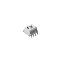
HCPL0500V Fairchild Semiconductor, HCPL0500V Datasheet

HCPL0500V
Specifications of HCPL0500V
Related parts for HCPL0500V
HCPL0500V Summary of contents
Page 1
... Open collector output Guaranteed performance over temperature: 0°C to 70°C U.L. recognized (File # E90700) VDE0884 recognized (file#136616) – approval pending for HCPL0530/0531/0453 – ordering option V, e.g., HCPL0500V BSI recognized (file# 8661, 8662) – HCPL0452/0500/0501 only Applications Line receivers Pulse transformer replacement ...
Page 2
... Peak Output Current O V Emitter-Base Reverse Voltage (HCPL0500/HCPL0501 only) EBR V Supply Voltage CC V Output Voltage O I Base Current (HCPL0500/HCPL0501 only Output power dissipation D ©2003 Fairchild Semiconductor Corporation HCPL0XXX Rev. 1.0 25°C unless otherwise specified) A Parameter 2 Value Units -40 to +125 °C -40 to +85 ° ...
Page 3
... Logic High Supply Current CCH Transfer Characteristics Symbol Parameter COUPLED CTR Current Tranfer Ratio (Note 1) V Logic Low Output Voltage OL *All typicals 25°C A ©2003 Fairchild Semiconductor Corporation HCPL0XXX Rev. 1.0 70°C unless otherwise specified) A Test Conditions Device I = 16mA 25° 16mA 10µ ...
Page 4
... V CM (Note 4) (Fig. 10) Isolation Characteristics Symbol Characteristics V Input-Output Isolation Voltage ISO R Isolation Resistance ISO C Isolation Capacitance ISO *All typicals 25°C A ©2003 Fairchild Semiconductor Corporation HCPL0XXX Rev. 1.0.4 (Continued 70°C unless otherwise specified 5V) CC Test Conditions = 25° 4. 16mA HCPL0500/0530 1. 16mA 25°C F ...
Page 5
... Device is considered a two terminal device: Pins and 4 are shorted together and Pins and 8 are shorted together. 6. 2500 VAC RMS for 1 minute duration is equivalent to 3000 VAC RMS for 1 second duration. ©2003 Fairchild Semiconductor Corporation HCPL0XXX Rev. 1.0 assure that the output will remain in a logic high state (i.e assure that the output will remain in a logic low state (i ...
Page 6
... OUTPUT VOLTAGE (V) O Fig. 5 Propagation Delay vs. Temperature 800 700 R = 4.1 K (TPLH) L 600 R = 4.1 K (TPLH) L 500 400 300 200 R = 1.9 K (TPHL 1.9 K (TPLH 100 0 -60 -40 - TEMPERATURE ( C) A ©2003 Fairchild Semiconductor Corporation HCPL0XXX Rev. 1.0.4 1.2 1.0 0.8 0 0.2 A 0.0 10 100 -60 1000 ...
Page 7
... F I/f < 100 Monitor Test Circuit for HCPL0452, HCPL0453, HCPL0500 and HCPL0501 I Noise F Shield Pulse Gen Test Circuit for HCPL0452, HCPL0453, HCPL0500 and HCPL0501 ©2003 Fairchild Semiconductor Corporation HCPL0XXX Rev. 1.0.4 Pulse V I Generator 5ns 10% DUTY CYCLE I/f < 100 0.1 F MONITOR 1.5 F ...
Page 8
... Package drawings are provided as a service to customers considering Fairchild components. Drawings may change in any manner without notice. Please note the revision and/or date on the drawing and contact a Fairchild Semiconductor representative to verify or obtain the most recent revision. Package specifications do not expand the terms of Fairchild’s worldwide terms and conditions, specifi ...
Page 9
... R2 R2 R2V R2V Marking Infomation ©2003 Fairchild Semiconductor Corporation HCPL0XXX Rev. 1.0.4 VDE 0884 (approval pending for HCPL0530, HCPL0531 & HCPL0534) Tape and reel (2500 units per reel) VDE 0884 (approval pending for HCPL0530, HCPL0531 & HCPL0534), Tape and reel (2500 units per reel) ...
Page 10
... Carrier Tape Specifications 3.50 0.20 0.30 MAX 8.3 0.10 0.1 MAX User Direction of Feed ©2003 Fairchild Semiconductor Corporation HCPL0XXX Rev. 1.0.4 8.0 0.10 2.0 0.05 Ø1.5 MIN 4.0 0.10 5.20 Ø1.5 6.40 0.20 10 1.75 0.10 5.5 0.05 12.0 0.3 0.20 ...
Page 11
... Liquidous Temperature (T Time (t ) Maintained Above (T L Peak Body Package Temperature Time (t ) within 5°C of 260°C P Ramp-down Rate (T Time 25°C to Peak Temperature ©2003 Fairchild Semiconductor Corporation HCPL0XXX Rev. 1.0.4 Max. Ramp-up Rate = 3°C/S Max. Ramp-down Rate = 6°C/S Tsmax Preheat Area Tsmin t s 120 240 Time 25° ...
Page 12
... TRADEMARKS The following includes registered and unregistered trademarks and service marks, owned by Fairchild Semiconductor and/or its global subsidiaries, and is not intended exhaustive list of all such trademarks. Auto-SPM™ F-PFS™ Build it Now™ FRFET CorePLUS™ Global Power Resource CorePOWER™ ...


