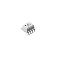
MOCD208R2M Fairchild Semiconductor, MOCD208R2M Datasheet - Page 2

MOCD208R2M
Manufacturer Part Number
MOCD208R2M
Description
Transistor Output Optocouplers 8-Pin Optocoupler 2Ch Phototransistor
Manufacturer
Fairchild Semiconductor
Datasheet
1.MOCD207VM.pdf
(9 pages)
Specifications of MOCD208R2M
Maximum Input Diode Current
60 mA
Maximum Reverse Diode Voltage
6 V
Output Device
Phototransistor
Output Type
DC
Configuration
2 Channel
Input Type
DC
Maximum Collector Emitter Voltage
70 V
Maximum Collector Emitter Saturation Voltage
0.4 V
Isolation Voltage
2500 Vrms
Current Transfer Ratio
125 %
Maximum Forward Diode Voltage
1.55 V
Maximum Collector Current
150 mA
Maximum Power Dissipation
250 mW
Maximum Operating Temperature
+ 100 C
Minimum Operating Temperature
- 40 C
Package / Case
SOIC-8 Narrow
Number Of Elements
2
Reverse Breakdown Voltage
6V
Forward Voltage
1.55V
Forward Current
60mA
Collector-emitter Voltage
70V
Package Type
SOIC W
Collector Current (dc) (max)
150mA
Power Dissipation
250mW
Collector-emitter Saturation Voltage
0.4V
Pin Count
8
Mounting
Surface Mount
Operating Temp Range
-40C to 100C
Operating Temperature Classification
Industrial
Lead Free Status / RoHS Status
Lead free / RoHS Compliant
Other names
MOCD208R2M_NL
Available stocks
Company
Part Number
Manufacturer
Quantity
Price
Company:
Part Number:
MOCD208R2M
Manufacturer:
Fairchil
Quantity:
6 000
Part Number:
MOCD208R2M
Manufacturer:
FAIRCHILD/仙童
Quantity:
20 000
©2003 Fairchild Semiconductor Corporation
MOCD207M, MOCD208M Rev. 1.0.6
Absolute Maximum Ratings
Stresses exceeding the absolute maximum ratings may damage the device. The device may not function or be
operable above the recommended operating conditions and stressing the parts to these levels is not recommended.
In addition, extended exposure to stresses above the recommended operating conditions may affect device reliability.
The absolute maximum ratings are stress ratings only.
EMITTER
DETECTOR
TOTAL DEVICE
Symbol
I
V
V
V
F
V
T
V
P
P
P
CEO
CBO
ECO
T
T
I
I
ISO
(pk)
stg
F
C
A
R
D
D
D
L
Forward Current – Continuous
Forward Current – Peak (PW = 100µs, 120pps)
Reverse Voltage
LED Power Dissipation @ T
Collector-Emitter Voltage
Collector-Base Voltage
Emitter-Collector Voltage
Collector Current-Continuous
Detector Power Dissipation @ T
Input-Output Isolation Voltage
Total Device Power Dissipation @ T
Ambient Operating Temperature Range
Storage Temperature Range
Lead Soldering Temperature (1/16” from case,
10 sec. duration)
Derate above 25°C
Derate above 25°C
(f = 60Hz, 1 min. Duration)
Derate above 25°C
(T
A
= 25°C unless otherwise specified)
Rating
A
= 25°C
(1, 2)
A
= 25°C
A
= 25°C
2
-40 to +100
-40 to +125
Value
2500
1.76
2.94
150
150
250
260
1.0
6.0
0.8
7.0
90
70
70
60
Vac(rms)
mW/°C
mW/°C
mW/°C
www.fairchildsemi.com
Unit
mW
mW
mW
mA
mA
°C
°C
°C
V
V
V
V
A


