4N40 Fairchild Semiconductor, 4N40 Datasheet
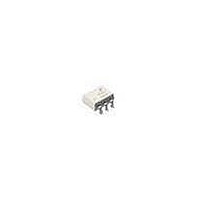
Triac & SCR Output Optocouplers DIP-6 PHOTO SCR

4N40

Manufacturer Part Number
4N40
Description
Triac & SCR Output Optocouplers DIP-6 PHOTO SCR
Manufacturer
Fairchild Semiconductor
Datasheet

Specifications of 4N40

Configuration
1
Maximum Continuous Output Current
300 mA
Maximum Input Current
60 mA
Maximum Operating Temperature
+ 100 C
Maximum Power Dissipation
450 mW
Maximum Reverse Diode Voltage
6 V
Maximum Turn-on Time
50 us
Minimum Operating Temperature
- 55 C
Output Type
AC
Package / Case
PDIP Black
Typical Input Voltage
1.1 V
Zero-crossing Circuit
No
Output Device
SCR
Isolation Voltage
5300 Vrms
Peak Output Voltage (vdrm)
400 V
Maximum Input Voltage
1.5 V
Maximum Output Voltage
280 VAC
Minimum Trigger Current
14 mA (Max)
Number Of Elements
1
Forward Voltage
1.5V
Repetitive Peak Off-state Volt
400V
Operating Temp Range
-55C to 100C
Output Current
300mA
Package Type
PDIP-B
Reverse Breakdown Voltage
6V
Mounting
Through Hole
Pin Count
6
Trigger Current
14mA
Zero Crossing Circuit
No
Operating Temperature Classification
Industrial
Forward Current
60mA
Power Dissipation
450mW
Lead Free Status / RoHS Status
Lead free / RoHS Compliant

Available stocks

Company
Part Number
Manufacturer
Quantity
Price
Part Number:
4N40
Manufacturer:
QTC
Quantity:
5 510
Part Number:
4N40
Manufacturer:
NS
Quantity:
5 510
Part Number:
4N40
Manufacturer:
FAIRCHILD/仙童
Quantity:
20 000
Company:
Part Number:
4N40
Quantity:
6 000
Part Number:
4N40SD
Manufacturer:
FAIRCHILD/仙童
Quantity:
20 000
Note
** Typical values at T
DS300381
DESCRIPTION
FEATURES
APPLICATIONS
TOTAL DEVICE
EMITTER
DETECTOR
The 4N39 and 4N40 have a gallium-arsenide infrared
emitting diode optically coupled with a light activated sil-
icon controlled rectifier in a dual in-line package.
• 10 A, T
• 25 W logic indicator lamp driver
• 400 V symmetrical transistor coupler
• Underwriters Laboratory (UL) recognized
• Low power logic circuits
• Telecommunications equipment
• Portable electronics
• Solid state relays
• Interfacing coupling systems of different potentials and impedances.
* Indicates JEDEC Registered Data
Parameter
*Storage Temperature
*Operating Temperature
*Lead Solder Temperature
*Total Device Power Dissipation (-55°C to 50 °C)
*Continuous Forward Current
*Reverse Voltage
*Forward Current - Peak (300 µs, 2% Duty Cycle)
*LED Power Dissipation (-55°C to 50 °C)
*Off-State And Reverse Voltage
*Peak Reverse Gate Voltage
*Direct On-State Current
*Surge On-State Current (100 µs)
*Peak Gate Current
*Detector Power Dissipation (-55°C to 50°C)
2001 Fairchild Semiconductor Corporation
Derate above 50°C
Derate above 50°C
Derate above 50°C
2
L compatible, solid state relay
2/27/01
A
= 25°C
File #E90700
Symbol
I
T
T
T
F
P
V
P
P
OPR
6
STG
SOL
(pk)
6
I
F
D
R
D
D
1 OF 8
PHOTO SCR OPTOCOUPLERS
1
1
Device
4N39
4N40
All
All
All
All
All
All
All
All
All
6
1
260 for 10 sec
-55 to +150
-55 to +100
Value
450
100
200
400
300
400
9.0
1.0
2.0
8.0
60
10
10
6
6
CATHODE
ANODE
www.fairchildsemi.com
N/C
4N39
1
2
3
SCHEMATIC
mW/°C
mW/°C
mW/°C
Units
mW
mW
mW
mA
mA
mA
°C
°C
°C
V
A
V
V
V
A
4N40
6 GATE
5
4
ANODE
CATHODE

Related parts for 4N40

4N40 Summary of contents

Page 1

... DESCRIPTION The 4N39 and 4N40 have a gallium-arsenide infrared emitting diode optically coupled with a light activated sil- icon controlled rectifier in a dual in-line package. FEATURES 2 • compatible, solid state relay • logic indicator lamp driver • 400 V symmetrical transistor coupler • Underwriters Laboratory (UL) recognized APPLICATIONS • ...

Page 2

... All All 50 4N39 200 4N40 400 4N39 200 4N40 400 All 4N39 4N40 150 4N39 4N40 150 All Min Typ** Max 4N39 4N40 ALL ALL ALL 500 Symbol Min Typ** Max V 5300 ISO ISO C 0.8 ISO 2/27/01 4N40 Unit 1 µ ...

Page 3

... AMBIENT TEMPERATURE ( ˚C) A Figure 4. Input Current To Trigger vs. Pluse Width NORMALIZED 50V 10K 25˚ 300 10K 27K 56K . 100 200 400 PULSE WIDTH (MICRO SECONDS) Figure 6. Input Characteristics I vs 1000 100 .01 .001 0.5 1.0 2.0 3 FORWARD VOLTAGE (VOLTS) AK www.fairchildsemi.com 4N40 120 1000 F ...

Page 4

... AMBIENT TEMP HALF-SINE WAVE AVGERAGE AMBIENT TEMP ANODE LEAD TEMP DC CURRENT 1/2 SINE WAVE AVERAGE 0.2 0.4 0 ON-STATE CURRENT (AMPERES) Figure 12. On-State Characteristics JUNCTION TEMPERATURE = 25 ˚C JUNCTION TEMPERATURE = 100 ˚C INCREASES TO FORWARD BREAKOVER VOLTAGE ON-STATE VOLTAGE (VOLTS ) T 2/27/01 4N40 40 100 DS300381 ...

Page 5

... SYMMETRICAL TRANSISTOR COUPLER Use of the high voltage PNP portion of the 4N40 provides a 400V transistor capable of conducting positive and negative signals with current transfer ratios of over 1%. This function is useful in remote instrumentation, high volt- age power supplies and test equipment ...

Page 6

... TYP 0.045 (1.14) 0.020 (0.51) MIN 0.016 (0.40) MIN 0.100 (2.54) 0.315 (8.00) TYP MIN 0.405 (10.30) MAX 0.070 (1.78) 0.060 (1.52) 0.100 (2.54) 0.295 (7.49) 0.030 (0.76) 2/27/01 4N40 0.016 (0.41) 0.008 (0.20) DS30381 ...

Page 7

... User Direction of Feed 4N39 4N40 Description Surface Mount Lead Bend Surface Mount; Tape and reel 0.4” Lead Spacing VDE 0884 VDE 0884, 0.4” Lead Spacing VDE 0884, Surface Mount VDE 0884, Surface Mount, Tape & ...

Page 8

MARKING INFORMATION Definitions Reflow Profile (Black Package, No Suffix) 300 250 225 C peak 200 150 Time above 183° C, 60–150 sec 100 50 Ramp C/sec 0 0 0.5 1 1.5 ...

Page 9

... TRADEMARKS The following are registered and unregistered trademarks Fairchild Semiconductor owns or is authorized to use and is not intended exhaustive list of all such trademarks.  ACEx™ FAST ActiveArray™ FASTr™ Bottomless™ FPS™ CoolFET™ FRFET™ CROSSVOLT™ GlobalOptoisolator™ ...

Related keywords