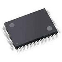
C8051F124TB Silicon Laboratories Inc, C8051F124TB Datasheet - Page 83

C8051F124TB
Manufacturer Part Number
C8051F124TB
Description
MCU, MPU & DSP Development Tools With C8051F124 MCU
Manufacturer
Silicon Laboratories Inc
Datasheet
1.C8051F120DK.pdf
(350 pages)
Specifications of C8051F124TB
Processor To Be Evaluated
C8051F12x and C8051F13x
Interface Type
USB
Lead Free Status / RoHS Status
Lead free / RoHS Compliant
- Current page: 83 of 350
- Download datasheet (2Mb)
VREF x (1023/1024)
VREF x (511/1024)
VREF x (511/512)
10-bit ADC0 Data Word appears in the ADC0 Data Word Registers as follows:
ADC0H[1:0]:ADC0L[7:0], if AD0LJST = 0
=
ADC0H[7:0]:ADC0L[7:6], if AD0LJST = 1
Example: ADC0 Data Word Conversion Map, AIN0.0 Input in Single-Ended Mode
Example: ADC0 Data Word Conversion Map, AIN0.0-AIN0.1 Differential Input Pair
For AD0LJST = 0:
Code
–VREF x (1/512)
VREF x (1/512)
AIN0.0–AIN0.1
AIN0.0–AGND
–VREF / 2
VREF / 2
VREF / 2
–VREF
(Volts)
(Volts)
=
0
0
(ADC0H[7:2] will be sign-extension of ADC0H.1 for a differential reading, otherwise
000000b).
(ADC0L[5:0] = 00b).
(AMX0CF = 0x00, AMX0SL = 0x00)
(AMX0CF = 0x01, AMX0SL = 0x00)
Vin
Figure 6.5. ADC0 Data Word Example
-------------- -
VREF
Gain
ADC0H:ADC0L
ADC0H:ADC0L
0xFF00 (–256d)
0xFE00 (–512d)
(AD0LJST = 0)
(AD0LJST = 0)
0xFFFF (–1d)
0x03FF
0x01FF
0x0000
0x01FF
0x0000
0x0200
0x0100
0x0001
2
n
; ‘n’ = 10 for Single-Ended; ‘n’= 9 for Differential.
Rev. 1.4
C8051F120/1/2/3/4/5/6/7
ADC0H:ADC0L
ADC0H:ADC0L
(AD0LJST = 1)
(AD0LJST = 1)
0xFFC0
0x7FC0
0xFFC0
0x7FC0
0xC000
0x8000
0x0000
0x4000
0x0040
0x0000
0x8000
C8051F130/1/2/3
83
Related parts for C8051F124TB
Image
Part Number
Description
Manufacturer
Datasheet
Request
R
Part Number:
Description:
SMD/C°/SINGLE-ENDED OUTPUT SILICON OSCILLATOR
Manufacturer:
Silicon Laboratories Inc
Part Number:
Description:
Manufacturer:
Silicon Laboratories Inc
Datasheet:
Part Number:
Description:
N/A N/A/SI4010 AES KEYFOB DEMO WITH LCD RX
Manufacturer:
Silicon Laboratories Inc
Datasheet:
Part Number:
Description:
N/A N/A/SI4010 SIMPLIFIED KEY FOB DEMO WITH LED RX
Manufacturer:
Silicon Laboratories Inc
Datasheet:
Part Number:
Description:
N/A/-40 TO 85 OC/EZLINK MODULE; F930/4432 HIGH BAND (REV E/B1)
Manufacturer:
Silicon Laboratories Inc
Part Number:
Description:
EZLink Module; F930/4432 Low Band (rev e/B1)
Manufacturer:
Silicon Laboratories Inc
Part Number:
Description:
I°/4460 10 DBM RADIO TEST CARD 434 MHZ
Manufacturer:
Silicon Laboratories Inc
Part Number:
Description:
I°/4461 14 DBM RADIO TEST CARD 868 MHZ
Manufacturer:
Silicon Laboratories Inc
Part Number:
Description:
I°/4463 20 DBM RFSWITCH RADIO TEST CARD 460 MHZ
Manufacturer:
Silicon Laboratories Inc
Part Number:
Description:
I°/4463 20 DBM RADIO TEST CARD 868 MHZ
Manufacturer:
Silicon Laboratories Inc
Part Number:
Description:
I°/4463 27 DBM RADIO TEST CARD 868 MHZ
Manufacturer:
Silicon Laboratories Inc
Part Number:
Description:
I°/4463 SKYWORKS 30 DBM RADIO TEST CARD 915 MHZ
Manufacturer:
Silicon Laboratories Inc
Part Number:
Description:
N/A N/A/-40 TO 85 OC/4463 RFMD 30 DBM RADIO TEST CARD 915 MHZ
Manufacturer:
Silicon Laboratories Inc
Part Number:
Description:
I°/4463 20 DBM RADIO TEST CARD 169 MHZ
Manufacturer:
Silicon Laboratories Inc


