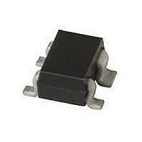
BF1105WR T/R NXP Semiconductors, BF1105WR T/R Datasheet - Page 3

BF1105WR T/R
Manufacturer Part Number
BF1105WR T/R
Description
RF MOSFET Small Signal TAPE-7 MOS-RFSS
Manufacturer
NXP Semiconductors
Datasheet
1.BF1105WR115.pdf
(15 pages)
Specifications of BF1105WR T/R
Configuration
Single Dual Gate
Transistor Polarity
N-Channel
Drain-source Breakdown Voltage
7 V
Gate-source Breakdown Voltage
7 V
Continuous Drain Current
0.03 A
Power Dissipation
200 mW
Maximum Operating Temperature
+ 150 C
Mounting Style
SMD/SMT
Minimum Operating Temperature
- 65 C
Package / Case
SOT-4
Application
VHF/UHF
Channel Type
N
Channel Mode
Enhancement
Drain Source Voltage (max)
7V
Power Gain (typ)@vds
38@5VdB
Noise Figure (max)
2.5dB
Frequency (max)
1GHz
Package Type
CMPAK
Pin Count
3 +Tab
Input Capacitance (typ)@vds
2.2@5V@Gate 1/1.6@5V@Gate 2pF
Output Capacitance (typ)@vds
1.2@5VpF
Reverse Capacitance (typ)
0.025@5VpF
Operating Temp Range
-65C to 150C
Mounting
Surface Mount
Number Of Elements
1
Power Dissipation (max)
200mW
Screening Level
Military
Lead Free Status / RoHS Status
Lead free / RoHS Compliant
Other names
BF1105WR,115
NXP Semiconductors
LIMITING VALUES
In accordance with the Absolute Maximum Rating System (IEC 134).
Note
1. Device mounted on a printed-circuit board.
1997 Dec 02
handbook, halfpage
V
I
I
I
P
T
T
SYMBOL
D
G1
G2
stg
j
DS
tot
N-channel dual-gate MOS-FETs
(mW)
P tot
250
200
150
100
50
0
0
drain-source voltage
drain current
gate 1 current
gate 2 current
total power dissipation
storage temperature
operating junction temperature
Fig.4 Power derating curve.
40
PARAMETER
80
120
T amb (°C)
MGM243
160
T
amb
80 C; note 1; see Fig.4
3
CONDITIONS
BF1105; BF1105R; BF1105WR
65
MIN.
7
30
10
10
200
+150
+150
Product specification
MAX.
V
mA
mA
mA
mW
C
C
UNIT


