HGTG27N120BN Fairchild Semiconductor, HGTG27N120BN Datasheet - Page 2
HGTG27N120BN
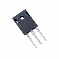
Manufacturer Part Number
HGTG27N120BN
Description
IGBT NPT N-CH 1200V 72A TO-247
Manufacturer
Fairchild Semiconductor
Datasheet
1.HGTG27N120BN.pdf
(8 pages)
Specifications of HGTG27N120BN
Igbt Type
NPT
Voltage - Collector Emitter Breakdown (max)
1200V
Vce(on) (max) @ Vge, Ic
2.7V @ 15V, 27A
Current - Collector (ic) (max)
72A
Power - Max
500W
Input Type
Standard
Mounting Type
Through Hole
Package / Case
TO-247-3
Configuration
Single
Collector- Emitter Voltage Vceo Max
1200 V
Collector-emitter Saturation Voltage
2.45 V
Maximum Gate Emitter Voltage
+/- 20 V
Continuous Collector Current At 25 C
72 A
Gate-emitter Leakage Current
+/- 250 nA
Power Dissipation
500 W
Maximum Operating Temperature
+ 150 C
Continuous Collector Current Ic Max
72 A
Minimum Operating Temperature
- 55 C
Mounting Style
Through Hole
Transistor Type
IGBT
Dc Collector Current
72A
Collector Emitter Voltage Vces
1.2kV
Power Dissipation Pd
500W
Collector Emitter Voltage V(br)ceo
1.2kV
Operating Temperature Range
-55°C To +150°C
Rohs Compliant
Yes
Lead Free Status / RoHS Status
Lead free / RoHS Compliant
Available stocks
Company
Part Number
Manufacturer
Quantity
Price
Company:

Part Number:
HGTG27N120BN
Manufacturer:
FAIRCHILD
Quantity:
12 500


Absolute Maximum Ratings
Collector to Emitter Voltage . . . . . . . . . . . . . . . . . . . . . . . . . . . . . . . . . . . . . . . . . . . . . .BV
Collector Current Continuous
Collector Current Pulsed (Note 1) . . . . . . . . . . . . . . . . . . . . . . . . . . . . . . . . . . . . . . . . . . . I
Gate to Emitter Voltage Continuous. . . . . . . . . . . . . . . . . . . . . . . . . . . . . . . . . . . . . . . . . V
Gate to Emitter Voltage Pulsed . . . . . . . . . . . . . . . . . . . . . . . . . . . . . . . . . . . . . . . . . . . .V
Switching Safe Operating Area at T
Power Dissipation Total at T
Power Dissipation Derating T
Forward Voltage Avalanche Energy (Note 2) . . . . . . . . . . . . . . . . . . . . . . . . . . . . . . . . . . . E
Operating and Storage Junction Temperature Range . . . . . . . . . . . . . . . . . . . . . . . . T
Maximum Lead Temperature for Soldering . . . . . . . . . . . . . . . . . . . . . . . . . . . . . . . . . . . . . T
Short Circuit Withstand Time (Note 3) at V
Short Circuit Withstand Time (Note 3) at V
CAUTION: Stresses above those listed in “Absolute Maximum Ratings” may cause permanent damage to the device. This is a stress only rating and operation of the
device at these or any other conditions above those indicated in the operational sections of this specification is not implied.
NOTES:
Electrical Specifications
©2004 Fairchild Semiconductor Corporation
Collector to Emitter Breakdown Voltage
Emitter to Collector Breakdown Voltage
Collector to Emitter Leakage Current
Collector to Emitter Saturation Voltage
Gate to Emitter Threshold Voltage
Gate to Emitter Leakage Current
Switching SOA
Gate to Emitter Plateau Voltage
On-State Gate Charge
Current Turn-On Delay Time
Current Rise Time
Current Turn-Off Delay Time
Current Fall Time
Turn-On Energy (Note 5)
Turn-On Energy (Note 5)
Turn-Off Energy (Note 4)
1. Pulse width limited by Max junction temperature.
2. I
3. V
At T
At T
CE
CE(PK)
C
C
= 25
= 110
= 30A, L = 400 H, T
o
= 960V, T
C . . . . . . . . . . . . . . . . . . . . . . . . . . . . . . . . . . . . . . . . . . . . . . . . . . . . . . . . . I
o
PARAMETER
C . . . . . . . . . . . . . . . . . . . . . . . . . . . . . . . . . . . . . . . . . . . . . . . . . . . . . . . I
J
= 125
C
J
C
= 25
= 125
o
> 25
C, R
o
J
C . . . . . . . . . . . . . . . . . . . . . . . . . . . . . . . . . . . . . . . . . P
o
T
o
G
C . . . . . . . . . . . . . . . . . . . . . . . . . . . . . . . . . . . . . . . . . .
= 150
C
C
T
= 3
= 25
C
= 25
GE
GE
o
o
C (Figure 2) . . . . . . . . . . . . . . . . . . . . . . . SSOA
HGTG27N120BN / HGT5A27N120BN
C, Unless Otherwise Specified
= 15V. . . . . . . . . . . . . . . . . . . . . . . . . . . . . .t
= 12V. . . . . . . . . . . . . . . . . . . . . . . . . . . . . .t
o
C, Unless Otherwise Specified
SYMBOL
V
V
Q
t
BV
BV
t
d(OFF)I
CE(SAT)
SSOA
GE(TH)
V
E
E
E
d(ON)I
I
I
G(ON)
GES
CES
GEP
ON1
ON2
OFF
t
t
CES
ECS
rI
fI
I
I
V
I
V
I
V
T
L = 200 H, V
I
I
V
IGBT and Diode at T
I
V
V
R
L = 1mH,
Test Circuit (Figure 18)
C
C
C
C
C
C
CE
GE
GE
J
GE
CE
CE
CE
G
= 250 A, V
= 10mA, V
= 27A,
= 250 A, V
= I
= 27A,
= 150
= 3
= 27A,
= 1200V
= 15V
= 20V
= 600V
= 960V,
= 15V,
C110
o
TEST CONDITIONS
C, R
, V
CE(PK)
CE
GE
GE
CE
G
= 3
= 0.5 BV
= 0V
= V
= 0V
GE
= 1200V
J
T
T
T
T
T
V
V
J
= 25
, T
C
C
C
C
C
GE
GE
V
GE
C110
GEM
= 25
= 125
= 150
= 25
= 150
CES
GES
CES
STG
C25
CM
= 15V
= 20V
SC
SC
o
AV
C,
D
= 15V,
L
o
o
C
C
o
o
o
C
C
C
HGTG27N120BN
150A at 1200V
-55 to 150
1200
MIN
150
15
1200
6
216
500
135
260
-
-
-
-
-
-
-
-
-
-
-
-
-
-
-
-
4.0
72
34
15
20
30
8
HGTG27N120BN / HGT5A27N12BN Rev. C2
TYP
2.45
300
270
350
195
3.8
6.6
9.2
2.2
2.7
2.3
24
20
80
-
-
-
-
-
-
MAX
250
325
420
240
120
2.7
4.2
250
3.3
2.8
30
25
4
-
-
-
-
-
-
-
UNITS
W/
mJ
o
o
W
V
A
A
A
V
V
C
C
UNITS
o
s
s
C
mA
nC
nC
mJ
mJ
mJ
nA
ns
ns
ns
ns
V
V
V
V
V
A
V
A
A
Related parts for HGTG27N120BN
Image
Part Number
Description
Manufacturer
Datasheet
Request
R

Part Number:
Description:
Fairchild Semiconductor [IGBT MODULE]
Manufacturer:
Fairchild Semiconductor
Datasheet:

Part Number:
Description:
Discrete Semiconductor Modules
Manufacturer:
Fairchild Semiconductor
Part Number:
Description:
Discrete Semiconductor Modules
Manufacturer:
Fairchild Semiconductor
Part Number:
Description:
This N-Channel MOSFET is produced using Fairchild Semiconductor’s advanced Power Trench® process
Manufacturer:
Fairchild Semiconductor
Datasheet:
Part Number:
Description:
This N-Channel MOSFET is produced using Fairchild Semiconductor’s advanced Power Trench® process
Manufacturer:
Fairchild Semiconductor
Datasheet:
Part Number:
Description:
This N-Channel MOSFET is produced using Fairchild Semiconductor’s advanced PowerTrench® process
Manufacturer:
Fairchild Semiconductor
Datasheet:
Part Number:
Description:
This N-Channel MOSFET is produced using Fairchild Semiconductor’s advanced PowerTrench® process
Manufacturer:
Fairchild Semiconductor
Datasheet:
Part Number:
Description:
This N-Channel MOSFET is produced using Fairchild Semiconductor’s advanced Power Trench® process
Manufacturer:
Fairchild Semiconductor
Datasheet:
Part Number:
Description:
This N-Channel logic Level MOSFETs are produced using Fairchild Semiconductor‘s advanced Power Trench® process that has been special tailored to minimize the on-state resistance and yet maintain superior switching performance
Manufacturer:
Fairchild Semiconductor
Datasheet:
Part Number:
Description:
This N-Channel MOSFET is produced using Fairchild Semiconductor’s advanced Power Trench® process
Manufacturer:
Fairchild Semiconductor
Datasheet:
Part Number:
Description:
This N-Channel SyncFET™ is produced using Fairchild Semiconductor’s advanced PowerTrench® process
Manufacturer:
Fairchild Semiconductor
Datasheet:
Part Number:
Description:
This N-Channel SyncFET™ is produced using Fairchild Semiconductor’s advanced PowerTrench® process
Manufacturer:
Fairchild Semiconductor
Datasheet:
Part Number:
Description:
This N-Channel SyncFET™ is produced using Fairchild Semiconductor’s advanced PowerTrench® process
Manufacturer:
Fairchild Semiconductor
Datasheet:
Part Number:
Description:
This N-Channel logic Level MOSFETs are produced using Fairchild Semiconductor‘s advanced Power Trench® process that has been special tailored to minimize the on-state resistance and yet maintain superior switching performance
Manufacturer:
Fairchild Semiconductor
Datasheet:
Part Number:
Description:
This N-Channel MOSFET is produced using Fairchild Semiconductor’s advanced Power Trench® process that has been especially tailored to minimize the on-state resistance and yet maintain superior switching performance
Manufacturer:
Fairchild Semiconductor
Datasheet: