FGH40N6S2D Fairchild Semiconductor, FGH40N6S2D Datasheet - Page 2
FGH40N6S2D
Manufacturer Part Number
FGH40N6S2D
Description
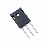
IGBT N-CH SMPS 600V 75A TO247
Manufacturer
Fairchild Semiconductor
Datasheet
1.FGH40N6S2D.pdf
(9 pages)
Specifications of FGH40N6S2D
Voltage - Collector Emitter Breakdown (max)
600V
Vce(on) (max) @ Vge, Ic
2.7V @ 15V, 20A
Current - Collector (ic) (max)
75A
Power - Max
290W
Input Type
Standard
Mounting Type
Through Hole
Package / Case
TO-247-3
Lead Free Status / RoHS Status
Lead free / RoHS Compliant
Igbt Type
-
Other names
FGH40N6S2D_NL
FGH40N6S2D_NL
FGH40N6S2D_NL
Available stocks
Company
Part Number
Manufacturer
Quantity
Price
Company:

Part Number:
FGH40N6S2D
Manufacturer:
FSC
Quantity:
6 000


©2002 Fairchild Semiconductor Corporation
Package Marking and Ordering Information
Electrical Characteristics
Off State Characteristics
On State Characteristics
Dynamic Characteristics
Switching Characteristics
Thermal Characteristics
NOTE:
V
Symbol
V
Q
t
t
BV
SSOA
t
t
d(OFF)I
d(OFF)I
CE(SAT)
V
E
E
E
E
E
E
R
2.
of the IGBT only. E
as the IGBT. The diode type is specified in figure 26.
3.
the input pulse and ending at the point where the collector current equals zero (I
JEDEC Standard No. 24-1 Method for Measurement of Power Device Turn-Off Switching Loss. This test method produc-
es the true total Turn-Off Energy Loss.
GE(TH)
d(ON)I
d(ON)I
I
I
V
Device Marking
G(ON)
CES
GES
GEP
ON1
ON2
OFF
ON1
ON2
OFF
t
t
t
t
t
EC
Values for two Turn-On loss conditions are shown for the convenience of the circuit designer. E
Turn-Off Energy Loss (E
CES
rr
rI
fI
rI
fI
JC
40N6S2D
Collector to Emitter Breakdown Voltage I
Collector to Emitter Leakage Current
Gate to Emitter Leakage Current
Collector to Emitter Saturation Voltage
Diode Forward Voltage
Gate Charge
Gate to Emitter Threshold Voltage
Gate to Emitter Plateau Voltage
Switching SOA
Current Turn-On Delay Time
Current Rise Time
Current Turn-Off Delay Time
Current Fall Time
Turn-On Energy (Note 2)
Turn-On Energy (Note 2)
Turn-Off Energy (Note 3)
Current Turn-On Delay Time
Current Rise Time
Current Turn-Off Delay Time
Current Fall Time
Turn-On Energy (Note 2)
Turn-On Energy (Note 2)
Turn-Off Energy (Note 3)
Diode Reverse Recovery Time
Thermal Resistance Junction-Case
ON2
Parameter
is the turn-on loss when a typical diode is used in the test circuit and the diode is at the same T
FGH40N6S2D
OFF
Device
) is defined as the integral of the instantaneous power loss starting at the trailing edge of
T
J
= 25°C unless otherwise noted
V
V
I
V
I
I
V
I
I
T
L = 100 H, V
IGBT and Diode at T
I
V
V
R
L = 200 H
Test Circuit - Figure 26
IGBT and Diode at T
I
V
V
R
L = 200 H
Test Circuit - Figure 26
I
I
IGBT
Diode
C
C
EC
C
C
C
CE
CE
EC
EC
CE
GE
GE
CE
J
CE
GE
CE
GE
G
G
Package
= 250 A, V
= 20A,
= 20A,
= 250 A, V
= 20A, V
TO-247
= 150°C, V
= 20A,
= 20A,
= 20A
= 3
= 3
= 1A, dI
= 20A, dI
= 15V
= 600V
= ± 20V
= 300V
= 390V,
= 15V,
= 390V,
= 15V,
Test Conditions
CE
EC
EC
CE
GE
CE
GE
/dt = 200A/ s
= 300V
/dt = 200A/ s
= 600V
= V
= 0
= 15V, R
T
T
T
T
V
V
J
J
J
J
GE
GE
GE
= 25°C
= 125°C
= 25°C
= 125°C
J
J
= 15V
= 20V
= 25°C,
= 125°C
G
= 3
Tape Width
CE
N/A
= 0A). All devices were tested per
Min
600
100
3.5
-
-
-
-
-
-
-
-
-
-
-
-
-
-
-
-
-
-
-
-
-
-
-
-
-
-
-
Typ
115
200
195
115
380
375
1.9
1.7
2.2
4.3
6.5
8.0
35
45
10
35
55
14
18
68
85
30
39
-
-
-
-
-
-
-
ON1
is the turn-on loss
±250
Max
0.43
1.25
250
260
105
450
600
2.0
2.7
2.0
2.6
5.0
8.0
42
55
85
35
48
-
-
-
-
-
-
-
-
-
-
-
Quantity
FGH40N6S2D RevA3
30
Units
°C/W
°C/W
mA
nA
nC
nC
ns
ns
ns
ns
ns
ns
ns
ns
ns
ns
V
V
V
V
V
V
A
A
J
J
J
J
J
J
J
Related parts for FGH40N6S2D
Image
Part Number
Description
Manufacturer
Datasheet
Request
R

Part Number:
Description:
Fairchild Semiconductor [IGBT MODULE]
Manufacturer:
Fairchild Semiconductor
Datasheet:

Part Number:
Description:
Discrete Semiconductor Modules
Manufacturer:
Fairchild Semiconductor
Part Number:
Description:
Discrete Semiconductor Modules
Manufacturer:
Fairchild Semiconductor
Part Number:
Description:
This N-Channel MOSFET is produced using Fairchild Semiconductor’s advanced Power Trench® process
Manufacturer:
Fairchild Semiconductor
Datasheet:
Part Number:
Description:
This N-Channel MOSFET is produced using Fairchild Semiconductor’s advanced Power Trench® process
Manufacturer:
Fairchild Semiconductor
Datasheet:
Part Number:
Description:
This N-Channel MOSFET is produced using Fairchild Semiconductor’s advanced PowerTrench® process
Manufacturer:
Fairchild Semiconductor
Datasheet:
Part Number:
Description:
This N-Channel MOSFET is produced using Fairchild Semiconductor’s advanced PowerTrench® process
Manufacturer:
Fairchild Semiconductor
Datasheet:
Part Number:
Description:
This N-Channel MOSFET is produced using Fairchild Semiconductor’s advanced Power Trench® process
Manufacturer:
Fairchild Semiconductor
Datasheet:
Part Number:
Description:
This N-Channel logic Level MOSFETs are produced using Fairchild Semiconductor‘s advanced Power Trench® process that has been special tailored to minimize the on-state resistance and yet maintain superior switching performance
Manufacturer:
Fairchild Semiconductor
Datasheet:
Part Number:
Description:
This N-Channel MOSFET is produced using Fairchild Semiconductor’s advanced Power Trench® process
Manufacturer:
Fairchild Semiconductor
Datasheet:
Part Number:
Description:
This N-Channel SyncFET™ is produced using Fairchild Semiconductor’s advanced PowerTrench® process
Manufacturer:
Fairchild Semiconductor
Datasheet:
Part Number:
Description:
This N-Channel SyncFET™ is produced using Fairchild Semiconductor’s advanced PowerTrench® process
Manufacturer:
Fairchild Semiconductor
Datasheet:
Part Number:
Description:
This N-Channel SyncFET™ is produced using Fairchild Semiconductor’s advanced PowerTrench® process
Manufacturer:
Fairchild Semiconductor
Datasheet:
Part Number:
Description:
This N-Channel logic Level MOSFETs are produced using Fairchild Semiconductor‘s advanced Power Trench® process that has been special tailored to minimize the on-state resistance and yet maintain superior switching performance
Manufacturer:
Fairchild Semiconductor
Datasheet:
Part Number:
Description:
This N-Channel MOSFET is produced using Fairchild Semiconductor’s advanced Power Trench® process that has been especially tailored to minimize the on-state resistance and yet maintain superior switching performance
Manufacturer:
Fairchild Semiconductor
Datasheet: