J176 Fairchild Semiconductor, J176 Datasheet - Page 10
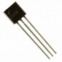
J176
Manufacturer Part Number
J176
Description
IC SWITCH P-CHAN 30V 50MA TO-92
Manufacturer
Fairchild Semiconductor
Datasheet
1.MMBFJ177.pdf
(12 pages)
Specifications of J176
Current - Drain (idss) @ Vds (vgs=0)
2mA @ 15V
Fet Type
P-Channel
Voltage - Breakdown (v(br)gss)
30V
Voltage - Cutoff (vgs Off) @ Id
1V @ 10nA
Resistance - Rds(on)
250 Ohm
Mounting Type
Through Hole
Package / Case
TO-92-3 (Standard Body), TO-226
Power - Max
350mW
Configuration
Single
Transistor Polarity
P-Channel
Power Dissipation
350 mW
Gate-source Breakdown Voltage
30 V
Gate-source Cutoff Voltage
4 V
Drain Current (idss At Vgs=0)
4 mA to 10 mA
Resistance Drain-source Rds (on)
250 Ohms
Maximum Operating Temperature
+ 150 C
Maximum Drain Gate Voltage
- 30 V
Minimum Operating Temperature
- 55 C
Mounting Style
Through Hole
Transistor Type
JFET
Breakdown Voltage Vbr
30V
Zero Gate Voltage Drain Current Idss
-2mA To -25mA
Gate-source Cutoff Voltage Vgs(off) Max
4V
Power Dissipation Pd
350mW
Rohs Compliant
Yes
Lead Free Status / RoHS Status
Lead free / RoHS Compliant
Other names
J176FS
Available stocks
Company
Part Number
Manufacturer
Quantity
Price
Company:

Part Number:
J176
Manufacturer:
SI/VISHAY
Quantity:
50 000
Company:
Part Number:
J176
Manufacturer:
FAIRCHILD
Quantity:
120 000
Part Number:
J176
Manufacturer:
MOTOROLA/µæ®µēśńĮŚµŗē
Quantity:
20 000
Company:
Part Number:
J176 DZ
Manufacturer:
FAIRCHILD
Quantity:
5 488
Company:
Part Number:
J176126
Manufacturer:
NXP Semiconductors
Quantity:
135


SOT-23 Tape and Reel Data, continued
SOT-23 Reel Configuration: Figure 4.0
Notes: A0, B0, and K0 dimensions are determined with respect to the EIA/Jedec RS-481
SOT-23 Embossed Carrier Tape
Configuration: Figure 3.0
Tape Size
8mm
8mm
B0
Pkg type
SOT-23
(8mm)
Dim A
max
rotational and lateral movement requirements (see sketches A, B, and C).
K0
7" Dia
13" Dia
T
Tc
Option
Wc
3.15
+/-0.10
Reel
A0
20 deg maximum component rotation
13" Diameter Option
2.77
+/-0.10
7.00
177.8
13.00
330
Dim A
B0
Sketch A (Side or Front Sectional View)
Component Rotation
8.0
+/-0.3
0.059
1.5
0.059
1.5
Dim B
W
1.55
+/-0.05
512 +0.020/-0.008
13 +0.5/-0.2
512 +0.020/-0.008
13 +0.5/-0.2
P0
D0
Dimensions are in inches and millimeters
Dim C
P1
1.125
+/-0.125
User Direction of Feed
D1
See detail AA
Dimensions are in millimeter
W2 max Measured at Hub
P2
1.75
+/-0.10
E1
Dim N
0.795
20.2
0.795
20.2
Dim D
W1 Measured at Hub
B0
A0
Sketch B (Top View)
Component Rotation
6.25
min
D0
E2
2.165
55
4.00
100
Dim N
A0
W3
3.50
+/-0.05
20 deg maximum
D1
F
0.331 +0.059/-0.000
8.4 +1.5/0
0.331 +0.059/-0.000
8.4 +1.5/0
Dim A
Typical
component
cavity
center line
Typical
component
center line
Dim D
Max
min
4.0
+/-0.1
Dim W1
P1
4.0
+/-0.1
7" Diameter Option
P0
DETAIL AA
Dim W2
0.567
14.4
0.567
14.4
1.30
+/-0.10
K0
Sketch C (Top View)
Component lateral movement
0.5mm
maximum
F
E1
E2
0.228
+/-0.013
0.311 – 0.429
7.9 – 10.9
0.311 – 0.429
7.9 – 10.9
Dim W3 (LSL-USL)
W
T
B Min
September 1999, Rev. C
Dim C
See detail AA
0.5mm
maximum
5.2
+/-0.3
Wc
0.06
+/-0.02
Tc
Related parts for J176
Image
Part Number
Description
Manufacturer
Datasheet
Request
R

Part Number:
Description:
Fairchild Semiconductor [IGBT MODULE]
Manufacturer:
Fairchild Semiconductor
Datasheet:

Part Number:
Description:
Discrete Semiconductor Modules
Manufacturer:
Fairchild Semiconductor
Part Number:
Description:
Discrete Semiconductor Modules
Manufacturer:
Fairchild Semiconductor
Part Number:
Description:
This N-Channel MOSFET is produced using Fairchild SemiconductorÆs advanced Power Trench« process
Manufacturer:
Fairchild Semiconductor
Datasheet:
Part Number:
Description:
This N-Channel MOSFET is produced using Fairchild SemiconductorÆs advanced Power Trench« process
Manufacturer:
Fairchild Semiconductor
Datasheet:
Part Number:
Description:
This N-Channel MOSFET is produced using Fairchild SemiconductorÆs advanced PowerTrench« process
Manufacturer:
Fairchild Semiconductor
Datasheet:
Part Number:
Description:
This N-Channel MOSFET is produced using Fairchild SemiconductorÆs advanced PowerTrench« process
Manufacturer:
Fairchild Semiconductor
Datasheet:
Part Number:
Description:
This N-Channel MOSFET is produced using Fairchild SemiconductorÆs advanced Power Trench« process
Manufacturer:
Fairchild Semiconductor
Datasheet:
Part Number:
Description:
This N-Channel logic Level MOSFETs are produced using Fairchild Semiconductoræs advanced Power Trench« process that has been special tailored to minimize the on-state resistance and yet maintain superior switching performance
Manufacturer:
Fairchild Semiconductor
Datasheet:
Part Number:
Description:
This N-Channel MOSFET is produced using Fairchild SemiconductorÆs advanced Power Trench« process
Manufacturer:
Fairchild Semiconductor
Datasheet:
Part Number:
Description:
This N-Channel SyncFETÖ is produced using Fairchild SemiconductorÆs advanced PowerTrench« process
Manufacturer:
Fairchild Semiconductor
Datasheet:
Part Number:
Description:
This N-Channel SyncFETÖ is produced using Fairchild SemiconductorÆs advanced PowerTrench« process
Manufacturer:
Fairchild Semiconductor
Datasheet:
Part Number:
Description:
This N-Channel SyncFETÖ is produced using Fairchild SemiconductorÆs advanced PowerTrench« process
Manufacturer:
Fairchild Semiconductor
Datasheet:
Part Number:
Description:
This N-Channel logic Level MOSFETs are produced using Fairchild Semiconductoræs advanced Power Trench« process that has been special tailored to minimize the on-state resistance and yet maintain superior switching performance
Manufacturer:
Fairchild Semiconductor
Datasheet:
Part Number:
Description:
This N-Channel MOSFET is produced using Fairchild SemiconductorÆs advanced Power Trench« process that has been especially tailored to minimize the on-state resistance and yet maintain superior switching performance
Manufacturer:
Fairchild Semiconductor
Datasheet: