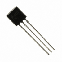
PN4392 Fairchild Semiconductor, PN4392 Datasheet - Page 2

PN4392
Manufacturer Part Number
PN4392
Description
TRANS SWITCH N-CH 30V .05A TO-92
Manufacturer
Fairchild Semiconductor
Datasheet
1.PN4391.pdf
(10 pages)
Specifications of PN4392
Current - Drain (idss) @ Vds (vgs=0)
25mA @ 20V
Fet Type
N-Channel
Voltage - Breakdown (v(br)gss)
30V
Voltage - Cutoff (vgs Off) @ Id
2V @ 1nA
Input Capacitance (ciss) @ Vds
14pF @ 20V
Resistance - Rds(on)
60 Ohm
Mounting Type
Through Hole
Package / Case
TO-92-3 (Standard Body), TO-226
Power - Max
625mW
Configuration
Single
Transistor Polarity
N-Channel
Power Dissipation
625 mW
Gate-source Breakdown Voltage
- 40 V
Gate-source Cutoff Voltage
- 5 V
Drain Current (idss At Vgs=0)
25 mA to 75 mA
Resistance Drain-source Rds (on)
60 Ohms
Maximum Operating Temperature
+ 150 C
Maximum Drain Gate Voltage
- 40 V
Minimum Operating Temperature
- 55 C
Mounting Style
Through Hole
Transistor Type
JFET
Breakdown Voltage Vbr
-30V
Gate-source Cutoff Voltage Vgs(off) Max
-5V
Power Dissipation Pd
625mW
Operating Temperature Range
-55°C To +150°C
No. Of Pins
3
Rohs Compliant
Yes
Lead Free Status / RoHS Status
Lead free / RoHS Compliant
Other names
PN4392FS
Available stocks
Company
Part Number
Manufacturer
Quantity
Price
Company:
Part Number:
PN4392
Manufacturer:
FSC
Quantity:
15 000
Company:
Part Number:
PN4392
Manufacturer:
SI/VISHAY
Quantity:
5
Company:
Part Number:
PN4392
Manufacturer:
FAIRCHILD
Quantity:
39 600
Company:
Part Number:
PN4392
Manufacturer:
VISHAY
Quantity:
4 000
Part Number:
PN4392
Manufacturer:
FSC
Quantity:
20 000
OFF CHARACTERISTICS
ON CHARACTERISTICS
SMALL-SIGNAL CHARACTERISTICS
V
I
V
V
I
I
V
r
r
C
C
SWITCHING CHARACTERISTICS
t
t
t
t
Symbol
GSS
D(off)
DSS
DS(
ds(on)
r
f
on
off
(BR)GSS
GS(off)
GS(f)
DS(
Electrical Characteristics
iss
rss
*
Pulse Test: Pulse Width 300 s, Duty Cycle 1.0%
on
on
)
)
Gate-Source Breakdown Voltage
Gate Reverse Current
Gate-Source Cutoff Voltage
Gate-Source Forward Voltage
Drain Cutoff Leakage Current
Zero-Gate Voltage Drain Current*
Drain-Source On Voltage
Drain-Source On Resistance
Drain-Source On Resistance
Input Capacitance
Reverse Transfer Capacitance
Rise Time
Fall Time
Turn-On Time
Turn-Off Time
Parameter
TA = 25°C unless otherwise noted
I
V
V
V
I
V
V
V
V
T
V
T
V
T
V
I
I
I
I
V
V
V
V
V
I
I
I
V
V
V
I
I
I
V
V
V
G
G
D
D
D
D
D(
D(
D(
D(
D(
D(
A
A
A
GS
GS
DS
DS
DS
DS
DS
DS
DS
DS
DS
DS
GS
GS
GS
GS(
GS(
GS(
GS(
GS(
GS(
= 12 mA, V
= 6.0 mA, V
= 3.0 mA, V
on
on
on
on)
on)
on)
= 1.0 A, V
= 1.0 mA, V
= 150 C
= 150 C
= 150 C
= 1.0 mA, V
= 20 V, V
= 20 V, V
= 20 V, V
= 20 V, I
= 20 V, V
= 20 V, V
= 20 V, V
= 20 V, V
)
)
)
off)
off)
off)
off)
off)
off)
= - 15 V, V
= - 15 V, V
= V
= 20, V
= - 12 V, f = 1.0 MHz
= - 7.0 V, f = 1.0 MHz
= - 5.0 V, f = 1.0 MHz
= 12 mA
= 3.0 mA
= 12 mA
= 6.0 mA
= 3.0 mA
= 6.0 mA
Test Conditions
= 12 V
= 6.0 V
= 3.0 V
= 12 V
= 6.0 V
= 3.0 V
GS
= 0, f= 1.0 kHz
GS
D
GS
GS
GS
GS
GS
GS
GS
DS
GS
DS
= 0, f = 1.0 MHz
= 1.0 nA
GS
GS
DS
DS
GS
= - 12 V,
= - 7.0 V,
= - 5.0 V,
= 0
= - 12 V
= - 7.0 V
= - 5.0 V
= 0
= 0
= 0
= 0
= 0
= 0
= 0, T
= 0
A
= 150 C
4391
4392
4393
4391
4392
4393
4391
4392
4393
4391
4392
4393
4391
4392
4393
4391
4392
4393
4391
4392
4393
4391
4392
4393
4391
4392
4393
4391
4392
4393
4391
4392
4393
4391
4392
4393
N-Channel Switch
Min
- 4.0
- 2.0
- 0.5
- 30
5.0
50
25
Max
- 1.0
- 0.2
- 5.0
- 3.0
- 10
150
100
100
0.4
0.4
0.4
1.0
0.1
0.1
0.1
0.2
0.2
0.2
3.5
3.5
3.5
5.0
5.0
5.0
75
30
30
60
30
60
14
15
20
30
15
15
15
20
35
50
(continued)
Units
mA
mA
mA
nA
nA
nA
nA
pF
pF
pF
pF
ns
ns
ns
ns
ns
ns
ns
ns
ns
ns
ns
ns
V
V
V
V
V
V
V
V
A
A
A
A
5


