FDC6561AN Fairchild Semiconductor, FDC6561AN Datasheet
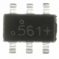
MOSFET N-CHAN DUAL 30V SSOT6

FDC6561AN

Manufacturer Part Number
FDC6561AN
Description
MOSFET N-CHAN DUAL 30V SSOT6
Manufacturer
Fairchild Semiconductor
Series
PowerTrench®r
Type
Power MOSFETr
Datasheet

Specifications of FDC6561AN

Fet Type
2 N-Channel (Dual)
Fet Feature
Logic Level Gate
Rds On (max) @ Id, Vgs
95 mOhm @ 2.5A, 10V
Drain To Source Voltage (vdss)
30V
Current - Continuous Drain (id) @ 25° C
2.5A
Vgs(th) (max) @ Id
3V @ 250µA
Gate Charge (qg) @ Vgs
3.2nC @ 5V
Input Capacitance (ciss) @ Vds
220pF @ 15V
Power - Max
700mW
Mounting Type
Surface Mount
Package / Case
6-SSOT, SuperSOT-6
Number Of Elements
2
Polarity
N
Channel Mode
Enhancement
Drain-source On-res
0.095Ohm
Drain-source On-volt
30V
Gate-source Voltage (max)
±20V
Drain Current (max)
2.5A
Power Dissipation
960mW
Output Power (max)
Not RequiredW
Frequency (max)
Not RequiredMHz
Noise Figure
Not RequireddB
Power Gain
Not RequireddB
Drain Efficiency
Not Required%
Operating Temp Range
-55C to 150C
Operating Temperature Classification
Military
Mounting
Surface Mount
Pin Count
6
Package Type
SuperSOT
Configuration
Dual
Transistor Polarity
N-Channel
Resistance Drain-source Rds (on)
0.095 Ohm @ 10 V
Forward Transconductance Gfs (max / Min)
5 S
Drain-source Breakdown Voltage
30 V
Gate-source Breakdown Voltage
+/- 20 V
Continuous Drain Current
2.5 A
Maximum Operating Temperature
+ 150 C
Mounting Style
SMD/SMT
Minimum Operating Temperature
- 55 C
Module Configuration
Dual
Continuous Drain Current Id
2.5A
Drain Source Voltage Vds
30V
On Resistance Rds(on)
95mohm
Rds(on) Test Voltage Vgs
10V
Rohs Compliant
Yes
Lead Free Status / RoHS Status
Lead free / RoHS Compliant
Other names
FDC6561ANTR

Available stocks

Company
Part Number
Manufacturer
Quantity
Price
Part Number:
FDC6561AN
Manufacturer:
Fairchild Semiconductor
Quantity:
61 880
Part Number:
FDC6561AN
Manufacturer:
FAIRCHILD
Quantity:
8 000
Part Number:
FDC6561AN
Manufacturer:
FAIRCHILD/仙童
Quantity:
20 000
Part Number:
FDC6561AN
0
Company:
Part Number:
FDC6561AN
Quantity:
42 093
Company:
Part Number:
FDC6561AN
Quantity:
5 000
Absolute Maximum Ratings
Symbol Parameter
V
V
I
P
T
THERMAL CHARACTERISTICS
R
R
© 1999 Fairchild Semiconductor Corporation
D
J
DSS
GSS
D
FDC6561AN
These N-Channel
produced using Fairchild Semiconductor's advanced
PowerTrench process that has been especially tailored
to minimize the on-state resistance and yet maintain
low gate charge for superior switching performance.
These devices are well suited for all applications where
small size is desireable but especially low cost DC/DC
conversion in battery powered systems.
General Description
,T
Dual N-Channel Logic Level PowerTrench
JA
JC
STG
SOT-23
SuperSOT -6
Drain-Source Voltage
Gate-Source Voltage - Continuous
Drain Current - Continuous
Maximum Power Dissipation
Operating and Storage Temperature Range
Thermal Resistance, Junction-to-Ambient
Thermal Resistance, Junction-to-Case
D1
S1
TM
- Pulsed
SuperSOT
Logic
D2
pin 1
TM
Level
-6
G1
T
A
S2
MOSFETs are
= 25°C unless otherwise note
SuperSOT
G2
(Note 1a)
(Note 1)
(Note 1a)
(Note 1b)
(Note 1c)
TM
-8
TM
2.5 A, 30 V. R
Very fast switching.
Low gate charge (2.1nC typical).
SuperSOT
standard SO-8); low profile (1mm thick).
Features
SO-8
MOSFET
TM
-6 package: small footprint (72% smaller than
R
6
5
4
DS(ON)
DS(ON)
-55 to 150
Ratings
0.96
±20
130
2.5
0.9
0.7
30
10
60
= 0.095
= 0.145
SOT-223
@ V
@ V
GS
GS
= 10 V
= 4.5 V
2
3
1
SOIC-16
FDC6561AN Rev.C
April 1999
Units
°C/W
°C/W
W
°C
V
V
A

Related parts for FDC6561AN

FDC6561AN Summary of contents

Page 1

... SO-8); low profile (1mm thick). TM SuperSOT -8 SO 25°C unless otherwise note A (Note 1a) (Note 1b) (Note 1c) (Note 1a) (Note 1) April 1999 = 0.095 @ DS(ON 0.145 @ V = 4.5 V DS(ON package: small footprint (72% smaller than SOIC-16 SOT-223 Ratings 30 ±20 2.5 10 0.96 0.9 0.7 -55 to 150 130 60 FDC6561AN Rev.C Units °C °C/W °C/W ...

Page 2

... C 0.005 in pad of 2oz copper. Min Typ Max 23 100 -100 1 1 0.082 0.095 125 C 0.122 0.152 J 0.113 0.145 10 5 220 2.3 3.2 0.7 1 0.9 1.3 0.75 0.78 1.2 (Note pad 180 C minimum pad. FDC6561AN Rev.C Units V o mV/ C µA µ mV guaranteed ...

Page 3

... Figure 2. On-Resistance Variation with Drain Current and Gate Voltage 1. 125° 25° GATE TO SOURCE VOLTAGE (V) GS Gate-to-Source Voltage 125°C A 25°C -55°C 0.2 0.4 0.6 0 BODY DIODE FORWARD VOLTAGE (V) SD Variation with Source Current and Temperature. FDC6561AN Rev 1.4 ...

Page 4

... Transient thermal response will change depending on the circuit board design. C iss C oss C rss = 0V 0 DRAIN TO SOURCE VOLTAGE (V) DS SINGLE PULSE R =180°C 25° 100 SINGLE PULSE TIME (SEC) Dissipation. R ( 180 °C P(pk ( Duty Cycle 100 300 FDC6561AN Rev.C 30 300 ...

Page 5

... TRADEMARKS The following are registered and unregistered trademarks Fairchild Semiconductor owns or is authorized to use and is not intended exhaustive list of all such trademarks. ACEx™ CoolFET™ CROSSVOLT™ CMOS FACT™ FACT Quiet Series™ ® FAST FASTr™ GTO™ ...

Related keywords