FDMA2002NZ Fairchild Semiconductor, FDMA2002NZ Datasheet
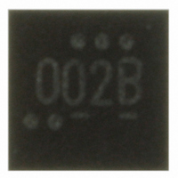
IC MOSFET N-CH DUAL MICROFET 2X2

FDMA2002NZ

Manufacturer Part Number
FDMA2002NZ
Description
IC MOSFET N-CH DUAL MICROFET 2X2
Manufacturer
Fairchild Semiconductor
Series
PowerTrench®r
Type
Power MOSFETr
Datasheet

Specifications of FDMA2002NZ

Fet Type
2 N-Channel (Dual)
Fet Feature
Logic Level Gate
Rds On (max) @ Id, Vgs
123 mOhm @ 2.9A, 4.5V
Drain To Source Voltage (vdss)
30V
Current - Continuous Drain (id) @ 25° C
2.9A
Vgs(th) (max) @ Id
1.5V @ 250µA
Gate Charge (qg) @ Vgs
3nC @ 4.5V
Input Capacitance (ciss) @ Vds
220pF @ 15V
Power - Max
650mW
Mounting Type
Surface Mount
Package / Case
6-MLP, 6-MicroFET™
Configuration
Dual
Transistor Polarity
N-Channel
Resistance Drain-source Rds (on)
0.123 Ohm @ 4.5 V
Drain-source Breakdown Voltage
30 V
Gate-source Breakdown Voltage
+/- 12 V
Continuous Drain Current
2.9 A
Power Dissipation
1500 mW
Maximum Operating Temperature
+ 150 C
Mounting Style
SMD/SMT
Minimum Operating Temperature
- 55 C
Number Of Elements
2
Polarity
N
Channel Mode
Enhancement
Drain-source On-res
0.123Ohm
Drain-source On-volt
30V
Gate-source Voltage (max)
±12V
Operating Temp Range
-55C to 150C
Operating Temperature Classification
Military
Mounting
Surface Mount
Pin Count
6
Package Type
MicroFET
Module Configuration
Dual
Continuous Drain Current Id
2.9A
Drain Source Voltage Vds
30V
On Resistance Rds(on)
123mohm
Rds(on) Test Voltage Vgs
1V
Rohs Compliant
Yes
Lead Free Status / RoHS Status
Lead free / RoHS Compliant
Other names
FDMA2002NZTR

Available stocks

Company
Part Number
Manufacturer
Quantity
Price
Part Number:
FDMA2002NZ
Manufacturer:
Fairchild Semiconductor
Quantity:
136 485
Part Number:
FDMA2002NZ
Manufacturer:
FAIRCHILD/仙童
Quantity:
20 000
FDMA2002NZ
Dual N-Channel PowerTrench MOSFET
General Description
This device is designed specifically as a single package
solution for dual switching requirements in cellular
handset
features two independent N-Channel MOSFETs with
low on-state resistance for minimum conduction losses.
The
performance for its physical size and is well suited to
linear mode applications.
20
R
R
R
R
Absolute Maximum Ratings
Symbol
V
V
I
P
T
Thermal Characteristics
Package Marking and Ordering Information
D
DS
GS
D
J
, T
JA
JA
JA
JA
Fairchild Semiconductor Corporation
Device Marking
STG
MicroFET
and
002
Drain-Source Voltage
Gate-Source Voltage
Drain Current – Continuous (T
Power Dissipation for Single Operation
Operating and Storage Temperature
Thermal Resistance, Junction-to-Ambient
other
2x2
MicroFET 2x2
ultra-portable
offers
– Continuous (T
– Pulsed
FDMA2002NZ
D1 G2 S2
exceptional
Device
PIN 1
D1
S1 G1
applications.
Parameter
D2
C
C
= 25°C, V
D2
= 25°C, V
thermal
T
A
=25
o
It
C unless otherwise noted
Reel Size
GS
GS
7’’
= 4.5V)
= 2.5V)
(Note 1a)
(Note 1b)
(Note 1d)
(Note 1c)
Features
2.9 A, 30 V R
Low profile – 0.8 mm maximum – in the new package
MicroFET 2x2 mm
HBM ESD protection level = 1.8kV (Note 3)
RoHS Compliant
Free from halogenated compounds and antimony
oxides
(Note 1a)
(Note 1b)
S1
G1
D2
1
2
3
193 (Single Operation)
R
83 (Single Operation)
145 (Dual Operation)
R
68 (Dual Operation)
DS(ON)
Tape width
DS(ON)
DS(ON)
8mm
= 140 m
= 123 m @ V
= 163 m
–55 to +150
Ratings
0.65
2.9
2.7
1.5
30
10
12
@ V
@ V
6
5
4
GS
GS
GS
May 20 0
= 3.0 V
= 4.5 V
= 2.5 V
D1
G2
S2
3000 units
FDMA2002NZ Rev B (W)
Quantity
Units
C/W
W
tm
V
V
A
t
C
tm
tm

Related parts for FDMA2002NZ

FDMA2002NZ Summary of contents

Page 1

... Reel Size 7’’ May 123 4.5 V DS(ON 140 3.0 V DS(ON 163 2.5 V DS(ON Ratings Units 2.9 2 1.5 W 0.65 –55 to +150 C 83 (Single Operation) 193 (Single Operation) C/W 68 (Dual Operation) 145 (Dual Operation) Tape width Quantity 8mm 3000 units FDMA2002NZ Rev B (W) tm ...

Page 2

... 1.0 MHz 4 GEN /dt = 100 A/μs F Min Typ Max Units mV/° ±10 A 0.4 1.0 1.5 V –3 mV 123 84 140 92 163 m 95 166 138 203 150 268 190 220 2.4 3.0 nC 0.35 nC 0.75 nC 2.9 A 0.9 1.2 V 0.8 1 FDMA2002NZ Rev B (W) ...

Page 3

... The diode connected between the gate and source serves only as protection against ESD. No gate overvoltage rating is implied. 2 oz. copper pad on a 1.5 x 1.5 in. board of FR-4 material b)173 C/W when mounted on a minimum pad copper. is guaranteed by design while R is determined by the d)151 C/W when o c)69 C/W when mounted mounted minimum pad pad copper. copper. FDMA2002NZ Rev B (W) ...

Page 4

... A 0.01 0.001 0.0001 2 0.2 Figure 6. Body Diode Forward Voltage Variation with Source Current and Temperature. = 2.0V GS 2.7V 2.9V 3.5V 4.0V 4. DRAIN CURRENT ( 1.45A 125 GATE TO SOURCE VOLTAGE ( -55 C 0.4 0.6 0.8 1 1.2 1 BODY DIODE FORWARD VOLTAGE (V) SD FDMA2002NZ Rev B ( 1.6 ...

Page 5

... Dimensional Outline and Pad Layout FDMA2002NZ Rev B (W) ...

Page 6

... TinyBuck™ TinyCalc™ ® TinyLogic TINYOPTO™ TinyPower™ TinyPWM™ TinyWire™ TriFault Detect™ TRUECURRENT™* µSerDes™ ® UHC Ultra FRFET™ UniFET™ VCX™ VisualMax™ XS™ Definition FDMA2002NZ Rev B (W) ®* ® Rev. I48 ...

Related keywords