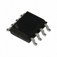
FDS3992 Fairchild Semiconductor, FDS3992 Datasheet - Page 7

FDS3992
Manufacturer Part Number
FDS3992
Description
MOSFET N-CH DUAL 100V 4.5A SO-8
Manufacturer
Fairchild Semiconductor
Series
PowerTrench®r
Type
Power MOSFETr
Datasheet
1.FDS3992.pdf
(11 pages)
Specifications of FDS3992
Fet Type
2 N-Channel (Dual)
Fet Feature
Standard
Rds On (max) @ Id, Vgs
62 mOhm @ 4.5A, 10V
Drain To Source Voltage (vdss)
100V
Current - Continuous Drain (id) @ 25° C
4.5A
Vgs(th) (max) @ Id
4V @ 250µA
Gate Charge (qg) @ Vgs
15nC @ 10V
Input Capacitance (ciss) @ Vds
750pF @ 25V
Power - Max
2.5W
Mounting Type
Surface Mount
Package / Case
8-SOIC (3.9mm Width)
Configuration
Dual Dual Drain
Transistor Polarity
N-Channel
Resistance Drain-source Rds (on)
0.062 Ohm @ 10 V
Drain-source Breakdown Voltage
100 V
Gate-source Breakdown Voltage
+/- 20 V
Continuous Drain Current
4.5 A
Power Dissipation
2500 mW
Maximum Operating Temperature
+ 150 C
Mounting Style
SMD/SMT
Minimum Operating Temperature
- 55 C
Number Of Elements
2
Polarity
N
Channel Mode
Enhancement
Drain-source On-res
0.062Ohm
Drain-source On-volt
100V
Gate-source Voltage (max)
±20V
Operating Temp Range
-55C to 150C
Operating Temperature Classification
Military
Mounting
Surface Mount
Pin Count
8
Package Type
SOIC N
Lead Free Status / RoHS Status
Lead free / RoHS Compliant
Other names
FDS3992
FDS3992TR
FDS3992TR
Available stocks
Company
Part Number
Manufacturer
Quantity
Price
Part Number:
FDS3992
Manufacturer:
FAIRCHILD/仙童
Quantity:
20 000
Part Number:
FDS3992-NL
Manufacturer:
FAIRCHILD/仙童
Quantity:
20 000
Company:
Part Number:
FDS3992_NL
Manufacturer:
FAIRCHILD
Quantity:
2 500
Part Number:
FDS3992_NL
Manufacturer:
FAIRCHILD/仙童
Quantity:
20 000
©2004 Fairchild Semiconductor Corporation
Thermal Resistance vs. Mounting Pad Area
The maximum rated junction temperature, T
thermal resistance of the heat dissipating path determines
the maximum allowable device power dissipation, P
application.
temperature, T
must be reviewed to ensure that T
Equation 1 mathematically represents the relationship and
serves as the basis for establishing the rating of the part.
In using surface mount devices such as the SO8 package,
the environment in which it is applied will have a significant
influence on the part’s current and maximum power
dissipation ratings. Precise determination of P
and influenced by many factors:
1. Mounting pad area onto which the device is attached and
2. The number of copper layers and the thickness of the
3. The use of external heat sinks.
4. The use of thermal vias.
5. Air flow and board orientation.
6. For non steady state applications, the pulse width, the
Fairchild provides thermal information to assist the
designer’s preliminary application evaluation. Figure 21
defines the R
copper (component side) area. This is for a horizontally
positioned FR-4 board with 1oz copper after 1000 seconds
of steady state power with no air flow. This graph provides
the necessary information for calculation of the steady state
junction
applications can be evaluated using the Fairchild device
Spice thermal model or manually utilizing the normalized
whether there is copper on one side or both sides of the
board.
board.
duty cycle and the transient thermal response of the part,
the board and the environment they are in.
P
DM
=
150
120
temperature
(
------------------------------ -
90
60
30
T
0
JM
10
R
θJA
-1
A
θJA
COPPER BOARD AREA - DESCENDING ORDER
0.04 in
0.28 in
0.52 in
0.76 in
1.00 in
–
(
Therefore
T
o
for the device as a function of the top
C), and thermal resistance R
A
)
2
2
2
2
2
or
Figure 22. Thermal Impedance vs Mounting Pad Area
the
power
application’s
JM
10
dissipation.
is never exceeded.
0
DM
JM
θJA
is complex
(EQ. 1)
t, RECTANGULAR PULSE DURATION (s)
, and the
DM
ambient
(
o
, in an
Pulse
C/W)
maximum transient thermal impedance curve.
Thermal resistances corresponding to other copper areas
can be obtained from Figure 21 or by calculation using
Equation 2. The area, in square inches is the top copper
area including the gate and source pads.
The transient thermal impedance (Z
varied top copper board area. Figure 22 shows the effect of
copper pad area on single pulse transient thermal
impedance. Each trace represents a copper pad area in
square inches corresponding to the descending list in the
graph. Spice and SABER thermal models are provided for
each of the listed pad areas.
Copper pad area has no perceivable effect on transient
thermal impedance for pulse widths less than 100ms. For
pulse widths less than 100ms the transient thermal
impedance is determined by the die and package.
Therefore, CTHERM1 through CTHERM5 and RTHERM1
through RTHERM5 remain constant for each of the thermal
models. A listing of the model component values is available
in Table 1.
10
R
1
θ JA
Figure 21. Thermal Resistance vs Mounting
200
150
100
50
=
0.001
64
+
-------------------------------
0.23
AREA, TOP COPPER AREA (in
0.01
26
+
Area
Pad Area
10
2
0.1
R
θJA
θJA
= 64 + 26/(0.23+Area)
) is also effected by
2
1
)
(EQ. 2)
FDS3992 Rev. B1
10
3
10


