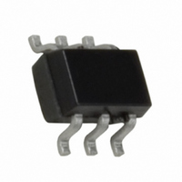
FDG6318PZ Fairchild Semiconductor, FDG6318PZ Datasheet - Page 2

FDG6318PZ
Manufacturer Part Number
FDG6318PZ
Description
MOSFET P-CH DUAL 20V SC70-6
Manufacturer
Fairchild Semiconductor
Specifications of FDG6318PZ
Fet Type
2 P-Channel (Dual)
Fet Feature
Logic Level Gate
Rds On (max) @ Id, Vgs
780 mOhm @ 500mA, 4.5V
Drain To Source Voltage (vdss)
20V
Current - Continuous Drain (id) @ 25° C
500mA
Vgs(th) (max) @ Id
1.5V @ 250µA
Gate Charge (qg) @ Vgs
1.62nC @ 4.5V
Input Capacitance (ciss) @ Vds
85.4pF @ 10V
Power - Max
300mW
Mounting Type
Surface Mount
Package / Case
SC-70-6, SC-88, SOT-363
Configuration
Dual
Transistor Polarity
P-Channel
Resistance Drain-source Rds (on)
0.78 Ohm @ 4.5 V
Forward Transconductance Gfs (max / Min)
1.1 S
Drain-source Breakdown Voltage
20 V
Gate-source Breakdown Voltage
+/- 12 V
Continuous Drain Current
0.5 A
Power Dissipation
300 mW
Maximum Operating Temperature
+ 150 C
Mounting Style
SMD/SMT
Minimum Operating Temperature
- 55 C
Lead Free Status / RoHS Status
Lead free / RoHS Compliant
Available stocks
Company
Part Number
Manufacturer
Quantity
Price
Company:
Part Number:
FDG6318PZ
Manufacturer:
FAIRCHILD
Quantity:
30 000
©2003 Fairchild Semiconductor Corporation
Electrical Characteristics
Off Characteristics
On Characteristics
Dynamic Characteristics
Switching Characteristics
Drain-Source Diode Characteristics
Notes:
1. R
B
I
I
V
r
C
C
C
Q
Q
Q
Q
t
t
t
t
t
t
V
t
Q
Symbol
DSS
GSS
DS(ON)
ON
d(ON)
r
d(OFF)
f
OFF
rr
GS(TH)
VDSS
ISS
OSS
RSS
SD
g(TOT)
g(-2.5)
gs
gd
RR
the center drain pad. R
JA
is the sum of the junction-to-case and case-to-ambient thermal resistance where the case thermal reference is defined as the solder mounting surface of
Drain to Source Breakdown Voltage
Zero Gate Voltage Drain Current
Gate to Source Leakage Current
Gate to Source Threshold Voltage
Drain to Source On Resistance
Input Capacitance
Output Capacitance
Reverse Transfer Capacitance
Total Gate Charge at -4.5V
Total Gate Charge at -2.5V
Gate to Source Gate Charge
Gate to Drain “Miller” Charge
Turn-On Time
Turn-On Delay Time
Rise Time
Turn-Off Delay Time
Fall Time
Turn-Off Time
Source to Drain Diode Voltage
Reverse Recovery Time
Reverse Recovered Charge
JC
is guaranteed by design while R
Parameter
(V
GS
= -4.5V)
T
A
= 25°C unless otherwise noted
CA
is determined by user’s board design. R
V
f = 1MHz
V
V
V
V
I
I
I
I
V
V
V
I
I
SD
SD
SD
D
D
D
DS
GS
GS
DD
GS
GS
GS
GS
= -250 A, V
= -0.5A, V
= -0.4A, V
= -0.5A
= -0.5A, dI
= -0.5A, dI
= -10V, V
= 16V , V
= 0V to -4.5V
= 0V to -2.5V
= -10V, I
= -4.5V, R
= 12V , V
= V
Test Conditions
DS
, I
D
GS
GS
D
GS
SD
SD
GS
GS
= -250 A
= -0.5A
GS
GS
= -4.5V
= -2.5V
/dt = 100A/ s
/dt = 100A/ s
= 0V,
= 0V
= 0V
= 120
= 0V
V
I
I
D
g
DD
= -0.5A
= 1.0mA
= -10V
JA
= 415
-0.65
o
Min
C/W when mounted on a 1inch
-20
-
-
-
-
-
-
-
-
-
-
-
-
-
-
-
-
-
-
-
-
85.4
24.9
8.83
1.08
0.67
0.21
0.33
580
910
-0.9
-0.9
Typ
10
13
40
24
-
-
-
-
-
-
-
1200
1.62
Max
-1.2
-1.5
1.0
780
35
96
22
16
-3
-
-
-
-
-
-
-
-
-
10
-
2
FDG6318PZ Rev. B
copper pad.
Units
nC
nC
nC
nC
nC
pF
pF
pF
ns
ns
ns
ns
ns
ns
ns
m
V
V
V
A
A


