FDC6318P Fairchild Semiconductor, FDC6318P Datasheet - Page 2
FDC6318P
Manufacturer Part Number
FDC6318P
Description
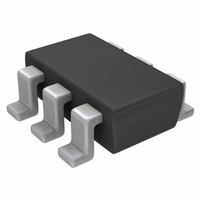
MOSFET P-CH DUAL 12V SSOT-6
Manufacturer
Fairchild Semiconductor
Series
PowerTrench®r
Datasheet
1.FDC6318P.pdf
(5 pages)
Specifications of FDC6318P
Fet Type
2 P-Channel (Dual)
Fet Feature
Logic Level Gate
Rds On (max) @ Id, Vgs
90 mOhm @ 2.5A, 4.5V
Drain To Source Voltage (vdss)
12V
Current - Continuous Drain (id) @ 25° C
2.5A
Vgs(th) (max) @ Id
1.5V @ 250µA
Gate Charge (qg) @ Vgs
8nC @ 4.5V
Input Capacitance (ciss) @ Vds
455pF @ 6V
Power - Max
700mW
Mounting Type
Surface Mount
Package / Case
6-SSOT, SuperSOT-6
Configuration
Dual
Transistor Polarity
P-Channel
Resistance Drain-source Rds (on)
0.09 Ohm @ 4.5 V
Forward Transconductance Gfs (max / Min)
8 S
Drain-source Breakdown Voltage
12 V
Gate-source Breakdown Voltage
+/- 8 V
Continuous Drain Current
2.5 A
Power Dissipation
960 mW
Maximum Operating Temperature
+ 150 C
Mounting Style
SMD/SMT
Minimum Operating Temperature
- 55 C
Module Configuration
Dual
Continuous Drain Current Id
2.5A
Drain Source Voltage Vds
-12V
On Resistance Rds(on)
90mohm
Rds(on) Test Voltage Vgs
-4.5V
Threshold Voltage Vgs Typ
700mV
Rohs Compliant
Yes
Lead Free Status / RoHS Status
Lead free / RoHS Compliant
Available stocks
Company
Part Number
Manufacturer
Quantity
Price

Part Number:
FDC6318P
Manufacturer:
ON/安森美
Quantity:
20 000
Company:
Part Number:
FDC6318P-NL
Manufacturer:
FAIRCHILD
Quantity:
2 120
Part Number:
FDC6318P-NL
Manufacturer:
FAIRCHILD/仙童
Quantity:
20 000


Notes:
1. R
Scale 1 : 1 on letter size paper
2. Pulse Test: Pulse Width < 300µs, Duty Cycle < 2.0%
Electrical Characteristics
Symbol
Off Characteristics
BV
∆BV
I
I
I
On Characteristics
V
∆V
R
I
g
Dynamic Characteristics
C
C
C
Switching Characteristics
t
t
t
t
Q
Q
Q
Drain–Source Diode Characteristics and Maximum Ratings
I
V
the drain pins. R
DSS
GSSF
GSSR
D(on)
d(on)
r
d(off)
f
S
FS
GS(th)
SD
θJA
DS(on)
iss
oss
rss
∆T
∆T
g
gs
gd
GS(th)
DSS
is the sum of the junction-to-case and case-to-ambient thermal resistance where the case thermal reference is defined as the solder mounting surface of
DSS
J
J
Drain–Source Breakdown Voltage
Breakdown Voltage Temperature
Coefficient
Zero Gate Voltage Drain Current
Gate–Body Leakage, Forward
Gate–Body Leakage, Reverse
Gate Threshold Voltage
Gate Threshold Voltage
Temperature Coefficient
Static Drain–Source
On–Resistance
On–State Drain Current
Forward Transconductance
Input Capacitance
Output Capacitance
Reverse Transfer Capacitance
Turn–On Delay Time
Turn–On Rise Time
Turn–Off Delay Time
Turn–Off Fall Time
Total Gate Charge
Gate–Source Charge
Gate–Drain Charge
Maximum Continuous Drain–Source Diode Forward Current
Drain–Source Diode Forward
Voltage
θJC
is guaranteed by design while R
a) 130 °C/W when
mounted on a 0.125
in
copper.
2
Parameter
pad of 2 oz.
(Note 2)
(Note 2)
θCA
is determined by the user's board design.
V
I
V
V
V
V
I
V
V
V
V
V
V
V
f = 1.0 MHz
V
V
V
V
V
T
D
D
A
GS
DS
GS
GS
DS
GS
GS
GS
GS
GS
DS
DS
DD
GS
DS
GS
GS
b) 140°C/W when mounted
= –250 µA, Referenced to 25°C
= –250 µA, Referenced to 25°C
= 25°C unless otherwise noted
= –4.5 V, I
= –10 V,
= V
= –5 V,
= –6 V,
= –6 V,
= 0 V,
= 8 V,
= –8 V,
= –4.5 V, I
= –2.5 V, I
= –1.8 V, I
= –4.5 V, V
= –6 V,
= –4.5 V, R
= –4.5 V
= 0 V,
on a .004 in
copper
Test Conditions
GS
,
2
D
pad of 2 oz
I
V
V
V
I
= –2.5A, T
I
V
I
I
I
D
D
D
D
D
D
D
D
S
GS
DS
DS
DS
GEN
GS
= –0.8 A
= –250 µA
= –250 µA
= –2.5 A
= –2 A
= –1.6 A
= –2.5 A
= –1 A,
= –2.5 A,
= 0 V
= 0 V
= 0 V
= –5 V
= 0 V,
= 6 Ω
J
=125°C
(Note 2)
Min
–0.4
–12
–6
c) 180°C/W when mounted on a
minimum pad.
Typ Max Units
–2.9
–0.7
–0.7
135
455
194
134
2.3
5.4
1.1
1.3
69
93
85
14
21
17
8
9
–100
–1.5
–0.8
–1.2
100
125
200
120
–1
90
18
25
34
31
8
FDC6318P Rev D (W)
mV/°C
mV/°C
mΩ
nC
nC
nC
µA
nA
nA
pF
pF
pF
ns
ns
ns
ns
V
V
A
S
A
V
Related parts for FDC6318P
Image
Part Number
Description
Manufacturer
Datasheet
Request
R

Part Number:
Description:
Fairchild Semiconductor [IGBT MODULE]
Manufacturer:
Fairchild Semiconductor
Datasheet:

Part Number:
Description:
Discrete Semiconductor Modules
Manufacturer:
Fairchild Semiconductor
Part Number:
Description:
Discrete Semiconductor Modules
Manufacturer:
Fairchild Semiconductor
Part Number:
Description:
This N-Channel MOSFET is produced using Fairchild Semiconductor’s advanced Power Trench® process
Manufacturer:
Fairchild Semiconductor
Datasheet:
Part Number:
Description:
This N-Channel MOSFET is produced using Fairchild Semiconductor’s advanced Power Trench® process
Manufacturer:
Fairchild Semiconductor
Datasheet:
Part Number:
Description:
This N-Channel MOSFET is produced using Fairchild Semiconductor’s advanced PowerTrench® process
Manufacturer:
Fairchild Semiconductor
Datasheet:
Part Number:
Description:
This N-Channel MOSFET is produced using Fairchild Semiconductor’s advanced PowerTrench® process
Manufacturer:
Fairchild Semiconductor
Datasheet:
Part Number:
Description:
This N-Channel MOSFET is produced using Fairchild Semiconductor’s advanced Power Trench® process
Manufacturer:
Fairchild Semiconductor
Datasheet:
Part Number:
Description:
This N-Channel logic Level MOSFETs are produced using Fairchild Semiconductor‘s advanced Power Trench® process that has been special tailored to minimize the on-state resistance and yet maintain superior switching performance
Manufacturer:
Fairchild Semiconductor
Datasheet:
Part Number:
Description:
This N-Channel MOSFET is produced using Fairchild Semiconductor’s advanced Power Trench® process
Manufacturer:
Fairchild Semiconductor
Datasheet:
Part Number:
Description:
This N-Channel SyncFET™ is produced using Fairchild Semiconductor’s advanced PowerTrench® process
Manufacturer:
Fairchild Semiconductor
Datasheet:
Part Number:
Description:
This N-Channel SyncFET™ is produced using Fairchild Semiconductor’s advanced PowerTrench® process
Manufacturer:
Fairchild Semiconductor
Datasheet:
Part Number:
Description:
This N-Channel SyncFET™ is produced using Fairchild Semiconductor’s advanced PowerTrench® process
Manufacturer:
Fairchild Semiconductor
Datasheet:
Part Number:
Description:
This N-Channel logic Level MOSFETs are produced using Fairchild Semiconductor‘s advanced Power Trench® process that has been special tailored to minimize the on-state resistance and yet maintain superior switching performance
Manufacturer:
Fairchild Semiconductor
Datasheet:
Part Number:
Description:
This N-Channel MOSFET is produced using Fairchild Semiconductor’s advanced Power Trench® process that has been especially tailored to minimize the on-state resistance and yet maintain superior switching performance
Manufacturer:
Fairchild Semiconductor
Datasheet: