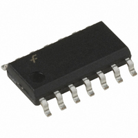
FDQ7238AS Fairchild Semiconductor, FDQ7238AS Datasheet

FDQ7238AS
Specifications of FDQ7238AS
Available stocks
Related parts for FDQ7238AS
FDQ7238AS Summary of contents
Page 1
... FDQ7238AS Dual Notebook Power Supply N-Channel PowerTrench General Description The FDQ7238AS is designed to replace two single SO- 8 MOSFETs power supplies. The high-side switch (Q1) is designed with specific emphasis on reducing switching losses while the low-side switch (Q2) is optimized to reduce conduction losses using TM Fairchild’s SyncFET technology ...
Page 2
... T = 125° 4 11 125° 1.0 MHz 15mV 1.0 MHz mV/°C 24 µA 500 1 5.6 mA µA 40 ±100 1.7 3 −3 mV/°C −4 7.2 8.7 mΩ 8.7 10.5 10 12 1530 pF 920 440 pF 190 160 pF 120 Ω 1.9 1.9 FDQ7238AS Rev A1 (X) ...
Page 3
... Type Min Typ Max Units 4 2 3 2.1 Q2 0.5 0.7 V 0.4 Q1 0.7 1 118°C/W when mounted on a minimum pad copper (Q1). d) 94°C/W when mounted on a minimum pad copper (Q2). FDQ7238AS Rev A1(X) ...
Page 4
... Figure 6. Body Diode Forward Voltage Variation with Source Current and Temperature. = 3.0V 3.5V 4.0V 4.5V 6. DRAIN CURRENT ( 125 GATE TO SOURCE VOLTAGE (V) GS Gate-to-Source Voltage 125 -55 C 0.2 0.4 0.6 0 BODY DIODE FORWARD VOLTAGE (V) SD FDQ7238AS Rev A1 (X) 10. ...
Page 5
... Figure 10. Single Pulse Maximum 0.01 0 TIME (sec 1MHz iss C oss DRAIN TO SOURCE VOLTAGE (V) DS SINGLE PULSE R = 94°C/W θ 25°C A 0.01 0 100 t , TIME (sec) 1 Power Dissipation. R ( θJA θ 94°C/W θJA P(pk (t) θ Duty Cycle 100 1000 FDQ7238AS Rev A1 ( 1000 ...
Page 6
... Schottky diode in parallel with a MOSFET. Figure 12 shows the reverse recovery characteristic of the FDQ7238AS Q2. TIME : 12nS/div Figure 12. FDQ7238AS SyncFET body diode reverse recovery characteristic. For comparison purposes, Figure 13 shows the reverse recovery characteristics of the body diode of an equivalent size MOSFET produced without SyncFET(FDS6670A) ...
Page 7
... C 0.01 0.001 0.0001 0 0.2 3 3.5 4 Figure 20. Body Diode Forward Voltage Variation with Source Current and Temperature. 4.0V 4.5V 6.0V 10. DRAIN CURRENT ( 5. 125 GATE TO SOURCE VOLTAGE ( 125 -55 C 0.4 0.6 0 BODY DIODE FORWARD VOLTAGE (V) SD FDQ7238AS Rev A1 ( 1.4 ...
Page 8
... Figure 24. Single Pulse Maximum 0.01 0 TIME (sec 1MHz iss C oss DRAIN TO SOURCE VOLTAGE (V) DS SINGLE PULSE R = 118°C/W θ 25° 100 t , TIME (sec) 1 Power Dissipation. R ( θJA θ 118 °C/W θJA P(pk (t) θ Duty Cycle 100 1000 FDQ7238AS Rev A1 (X) 30 1000 ...
Page 9
... Fairchild Semiconductor. The datasheet is for reference information only. ® The Power Franchise tm TinyBoost™ TinyBuck™ ® TinyLogic TINYOPTO™ TinyPower™ TinyPWM™ TinyWire™ µSerDes™ ® UHC Ultra FRFET™ UniFET™ VCX™ VisualMax™ Definition Rev. I34 FDQ7238AS Rev.A1(X) ...


