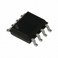
FDS9933 Fairchild Semiconductor, FDS9933 Datasheet - Page 4

FDS9933
Manufacturer Part Number
FDS9933
Description
MOSFET P-CH DUAL 20V 5A 8SOIC
Manufacturer
Fairchild Semiconductor
Series
PowerTrench®r
Datasheet
1.FDS9933.pdf
(5 pages)
Specifications of FDS9933
Fet Type
2 P-Channel (Dual)
Fet Feature
Logic Level Gate
Rds On (max) @ Id, Vgs
55 mOhm @ 3.2A, 4.5V
Drain To Source Voltage (vdss)
20V
Current - Continuous Drain (id) @ 25° C
5A
Vgs(th) (max) @ Id
1.2V @ 250µA
Gate Charge (qg) @ Vgs
20nC @ 4.5V
Input Capacitance (ciss) @ Vds
825pF @ 10V
Power - Max
900mW
Mounting Type
Surface Mount
Package / Case
8-SOIC (3.9mm Width)
Lead Free Status / RoHS Status
Lead free / RoHS Compliant
Available stocks
Company
Part Number
Manufacturer
Quantity
Price
Company:
Part Number:
FDS9933
Manufacturer:
FAIRCHILD
Quantity:
1
Part Number:
FDS9933-NL
Manufacturer:
FAIRCHILD/仙童
Quantity:
20 000
Company:
Part Number:
FDS9933A
Manufacturer:
FSC
Quantity:
50 000
Company:
Part Number:
FDS9933A
Manufacturer:
FSC
Quantity:
4 773
Part Number:
FDS9933A
Manufacturer:
FAIRCHILD/仙童
Quantity:
20 000
Company:
Part Number:
FDS9933A-NL
Manufacturer:
FSC
Quantity:
50 000
Company:
Part Number:
FDS9933A-NL
Manufacturer:
DIODES
Quantity:
3 000
Part Number:
FDS9933A-NL
Manufacturer:
FAIRCHILD/仙童
Quantity:
20 000
Part Number:
FDS9933A_NL
Manufacturer:
FAIRCHILD/仙童
Quantity:
20 000
Part Number:
FDS9933BZ
Manufacturer:
FAIRCHILD/仙童
Quantity:
20 000
Typical Characteristics:
5
4
3
2
1
0
0.01
Figure 9. Maximum Safe Operating Area.
100
0.1
10
0
Figure 7. Gate Charge Characteristics.
1
0.1
I
D
0.001
= -5A
R
0.01
0.1
DS(ON)
SINGLE PULSE
R
0.0001
1
V
JA
T
GS
A
= 135
LIMIT
= 25
= -4.5V
2
D = 0.5
0.2
o
0.1
o
0.05
C/W
C
0.02
-V
0.01
DS
, DRAIN-SOURCE VOLTAGE (V)
Q
g
1
, GATE CHARGE (nC)
SINGLE PULSE
4
DC
0.001
Thermal characterization performed using the conditions described in Note 1c.
Transient thermal response will change depending on the circuit board design.
10s
Figure 11. Transient Thermal Response Curve.
1s
100ms
6
V
10ms
DS
10
= -4V
1ms
0.01
-6V
100 s
8
-8V
100
10
0.1
t
1
, TIME (sec)
1600
1200
800
400
50
40
30
20
10
Figure 8. Capacitance Characteristics.
0
0.001
0
0
Figure 10. Single Pulse Maximum
1
C
rss
0.01
4
-V
Power Dissipation.
DS
, DRAIN TO SOURCE VOLTAGE (V)
0.1
C
10
oss
t
8
1
, TIME (sec)
1
Duty Cycle, D = t
P(pk)
T
R
J
R
JA
- T
12
JA
(t) = r(t) * R
100
A
= 135
C
10
= P * R
t
1
iss
t
2
SINGLE PULSE
R
o
C/W
JA
T
A
JA
= 135°C/W
1
FDS9933 Rev C
16
= 25°C
JA
(t)
100
/ t
2
f = 1 MHz
V
GS
1000
= 0 V
1000
20


